Electronic circuits do not operate in an electromagnetic vacuum. Every switching transistor, motor, power converter, cable, PCB trace, connector, and enclosure exists within an electromagnetic environment. Whenever changing voltages and currents interact with surrounding conductors or fields, unwanted electrical energy can be coupled from one part of a system to another. This unwanted interaction is commonly described as electromagnetic interference (EMI).
EMI is not limited to radio-frequency equipment. A switching regulator can inject noise into an analog sensor, a motor cable can disturb a communication line, a rapidly switching digital trace can couple into a neighboring trace, and a poorly terminated cable shield can allow radio-frequency energy to enter or leave an enclosure. The physical mechanisms are different, but they all belong to the same electromagnetic-interference problem.
Electromagnetic compatibility (EMC) is the broader engineering discipline concerned with making electronic equipment operate correctly in its electromagnetic environment without generating unacceptable interference to other equipment. EMI describes the unwanted interference itself; EMC describes the ability of the complete system to coexist with that interference environment.

What Is EMI?
Electromagnetic interference is unwanted electromagnetic energy that disturbs the normal operation of an electrical or electronic circuit. The interference may appear as an unwanted voltage, current, electromagnetic field, or combination of these effects.
A useful engineering model is to think of every EMI problem as having three essential elements: a source, a coupling path, and a victim.
EMI Source → Coupling Path → Victim Circuit
The source generates unwanted electromagnetic energy. The coupling path provides a mechanism through which that energy reaches another circuit. The victim is the circuit or component whose operation is disturbed by the interference.
This model is extremely useful because an EMI problem can often be solved by changing any one of these three elements. The source can be reduced, the coupling path can be interrupted or weakened, or the victim can be made less sensitive.
What Is EMC?
Electromagnetic compatibility describes the ability of equipment to function satisfactorily in its intended electromagnetic environment while not producing excessive electromagnetic disturbance for other equipment operating in the same environment.
EMC therefore has two complementary sides. A product must have sufficient immunity to electromagnetic disturbances, while its own emissions must remain within the applicable limits for the intended application.
                    EMC
                     │
          ┌──────────┴──────────┐
          ↓                     ↓
   Emissions Control       Immunity
   "Do not disturb"        "Do not fail"
This is why EMC engineering cannot be reduced to adding a shield after a product has already been designed. EMC performance is influenced by circuit topology, current loops, PCB layout, filtering, grounding and bonding, cable construction, enclosure design, connector interfaces, and the physical arrangement of the complete product.
EMI and EMC: What Is the Difference?
The terms EMI and EMC are closely related, but they describe different levels of the same engineering problem. EMI refers to unwanted electromagnetic disturbance, while EMC refers to the ability of equipment to coexist with electromagnetic disturbances within the intended environment.
| Term | Meaning | Engineering Question |
|---|---|---|
| EMI | Unwanted electromagnetic interference | What unwanted energy is disturbing the circuit? |
| EMC | Electromagnetic compatibility | Can the equipment operate correctly without causing unacceptable disturbance? |
| Emission | Electromagnetic energy produced by equipment | How much interference is the product generating? |
| Immunity | Resistance to external electromagnetic disturbance | How well does the product tolerate interference? |
Two Fundamental Ways EMI Travels
From a system-design perspective, EMI is commonly divided into conducted interference and radiated interference. The distinction is based on the dominant path by which unwanted energy reaches the victim circuit.
Conducted EMI
Conducted EMI travels through physical conductors. The unwanted current or voltage may propagate through power wiring, signal wiring, ground connections, cable shields, PCB traces, connector structures, or other conductive paths.
A switching regulator provides a simple example. Rapid current changes at the switching node can generate high-frequency components that propagate through the input or output wiring. Those components can then reach a sensitive circuit elsewhere in the system.
Conducted interference can therefore exist even when two circuits have no direct signal connection. A shared supply or return path may be enough to transfer the disturbance.
Radiated EMI
Radiated EMI reaches the victim predominantly through electromagnetic fields rather than a direct conductive connection. A rapidly changing current loop on a PCB, a motor cable, an enclosure opening, or a poorly controlled high-speed interconnect can become an efficient source of electromagnetic radiation.
The same physical system can also work in the opposite direction. A cable or circuit that behaves as a receiving structure can pick up an external electromagnetic field and convert part of that field into an unwanted electrical signal.
Conducted and Radiated EMI Are Connected
It is tempting to treat conducted and radiated EMI as completely separate problems, but real systems often contain both mechanisms. A rapidly changing current can create a conducted disturbance first and then produce radiated fields because the associated current loop has significant area. Likewise, an external field can couple into a cable and then propagate through the cable as a conducted disturbance.
This is why troubleshooting EMI requires examining the complete source-to-victim path rather than simply asking whether the noise is “conducted” or “radiated.” The two mechanisms can transform into one another as the interference propagates through the system.
Common-Mode and Differential-Mode Interference
Another fundamental classification is based on how interference appears on a pair of conductors. This distinction is particularly important for power systems, communication cables, differential interfaces, and PCB signal paths.
Differential-Mode Noise
Differential-mode noise appears as an unwanted voltage difference between two conductors. If the intended differential signal is represented by the difference between two conductor voltages, any additional unequal disturbance directly changes the measured signal.
V_{DM}=V_1-V_2Differential-mode interference is particularly important because it directly enters the signal measurement. Filtering, balanced transmission, proper impedance control, and careful source and return-path design are common methods used to reduce it.
Common-Mode Noise
Common-mode noise appears approximately in the same direction on multiple conductors relative to a reference. For two conductors, it can be represented by their average voltage:
V_{CM}=\frac{V_1+V_2}{2}A differential receiver can reject a portion of common-mode interference because it responds primarily to the voltage difference between its inputs. The degree of rejection is determined by the receiver’s common-mode rejection performance and, critically, by how well the physical interconnect preserves balance.
Why EMI Becomes More Difficult as Signal Edges Become Faster
EMI is not determined solely by the clock frequency printed on a datasheet. A digital waveform with a fast transition contains significant high-frequency spectral components even when its repetition frequency is comparatively low.
This is why a circuit operating at a moderate clock frequency can still behave like a high-frequency electromagnetic source. The important parameters include rise time, fall time, interconnect length, loop geometry, impedance, and the frequency-dependent behavior of the surrounding structures.
As transition times decrease, parasitic inductance and capacitance become increasingly important. A trace that behaved like an ordinary wire in a slow circuit can begin to behave as a transmission line, while a short current loop can become an effective source of unwanted electromagnetic radiation.
The Source–Path–Victim Model
A practical EMI investigation can be organized around three questions:
- What is generating the interference?
- How is the interference coupling into the victim?
- Why is the victim sensitive to that disturbance?
This approach prevents a common engineering mistake: treating a symptom rather than the actual coupling mechanism. For example, adding a capacitor to a noisy signal may reduce one observed symptom, but if the underlying problem is an excessively large current loop or a poorly terminated cable shield, the circuit may remain vulnerable under different operating conditions.
Where EMI and EMC Connect to the Rest of Electronics Design
EMI and EMC are not isolated subjects. They connect directly to shielding, twisted-pair transmission, differential signaling, grounding, filtering, cable routing, PCB layout, transmission lines, power integrity, and signal integrity.
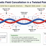
For example, a twisted pair reduces magnetic coupling by controlling conductor geometry. A differential receiver can reject common-mode interference. A shield can reduce electromagnetic coupling into or out of a cable. A filter can attenuate unwanted frequency components. A continuous reference plane can provide a controlled return path for high-frequency current.
The individual techniques are therefore parts of one larger engineering problem: controlling the generation, propagation, coupling, and susceptibility of unwanted electromagnetic energy.
EMI and EMC Topics for Deeper Study
The broad concepts introduced here will be developed in dedicated CircuitFeed articles so that each mechanism can be examined without mixing unrelated design problems together.
- EMI Protection and Reduction — practical methods for reducing interference at the source, coupling path, and victim.
- EMI Shielding — how conductive and magnetic barriers reduce electromagnetic coupling.
- Capacitive Coupling — electric-field coupling between conductors.
- Inductive Coupling — magnetic-field coupling caused by changing current.
- Common-Mode Noise — generation, propagation, and rejection of common-mode interference.
- Differential-Mode Noise — unwanted voltage differences that directly disturb a signal.
- Common-Mode Chokes — magnetic components used to attenuate common-mode currents.
- EMI Filtering — capacitors, inductors, ferrites, and filter networks.
- EMI Grounding and Bonding — controlling high-frequency current paths and reference connections.
- EMC Testing — emissions, immunity, and system-level electromagnetic compatibility.