
A square wave generator is one of the most fundamental oscillator circuits used throughout electronics. From blinking LEDs and digital clock sources to timing circuits and pulse generators, square waves form the basis of countless electronic systems. While integrated circuits such as the NE555 timer or CMOS logic gates are commonly used to generate these signals, it is equally possible to produce stable oscillations using only two MOSFETs, a pair of resistors, and two capacitors.
The circuit presented in this article is a MOSFET astable multivibrator built with two 2N7000 N-channel enhancement MOSFETs. operates on VCC 12V DC. Unlike a monostable circuit that produces a single pulse after being triggered, an astable multivibrator continuously switches between two states without any external clock. The result is a pair of complementary square-wave outputs that are exactly 180° out of phase with each other.
Although the circuit appears deceptively simple, it demonstrates several important electronic principles including RC timing, positive feedback, MOSFET switching, capacitor charging, regenerative action, and self-sustaining oscillation. Understanding how this circuit works provides an excellent foundation for learning more advanced oscillator designs, switching regulators, PWM generators, and digital timing circuits.
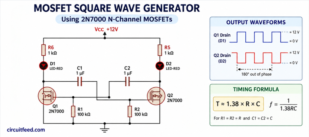
Circuit Overview
This oscillator consists of only a few inexpensive components, yet it produces continuous square-wave outputs without requiring any integrated circuit or microcontroller. Two identical MOSFETs alternately switch between the ON and OFF states while two cross-coupled capacitors provide regenerative feedback. As one transistor turns ON, it forces the opposite transistor OFF. After a short delay determined by the RC network, the situation reverses automatically. This process repeats indefinitely as long as power is applied.
The drains of both MOSFETs act as the output terminals. Because only one transistor conducts at any instant, one drain remains close to the supply voltage while the opposite drain is pulled near ground potential. Consequently, the outputs form complementary square waves that are particularly useful in timing applications, LED flashers, logic testing, and clock generation.
Components Used
| Reference | Value | Purpose |
|---|---|---|
| Q1, Q2 | 2N7000 | N-channel enhancement MOSFET |
| R1, R2 | 100 kΩ | Gate discharge resistors |
| R5, R6 | 1 kΩ | Drain load resistors |
| C1, C2 | 1 µF | Timing capacitors |
| D1, D2 | LED | Output indicators |
| VCC | 12 V DC | Power supply |
Why Use the 2N7000 MOSFET?
The 2N7000 has remained one of the most popular small-signal MOSFETs for decades because it combines low cost, high input impedance, fast switching speed, and wide availability. Unlike bipolar junction transistors that require continuous base current, a MOSFET is primarily a voltage-controlled device. Once the gate capacitance has been charged, almost no steady-state gate current is required. This characteristic allows the timing capacitors in the oscillator to operate with minimal loading, resulting in clean transitions and efficient switching.
The device is capable of operating from relatively low gate voltages and is well suited for low-frequency oscillator circuits such as this one. For hobbyists, students, and practicing engineers, the 2N7000 is often the first MOSFET selected when designing experimental switching circuits or timing generators.
How Does This MOSFET Square Wave Generator Work?
At first glance, both halves of the circuit appear perfectly symmetrical. If every component were absolutely identical, it might seem impossible for either MOSFET to turn on before the other. However, no electronic component is perfectly matched. Tiny manufacturing tolerances cause one transistor to conduct a fraction of a microsecond earlier than its counterpart.
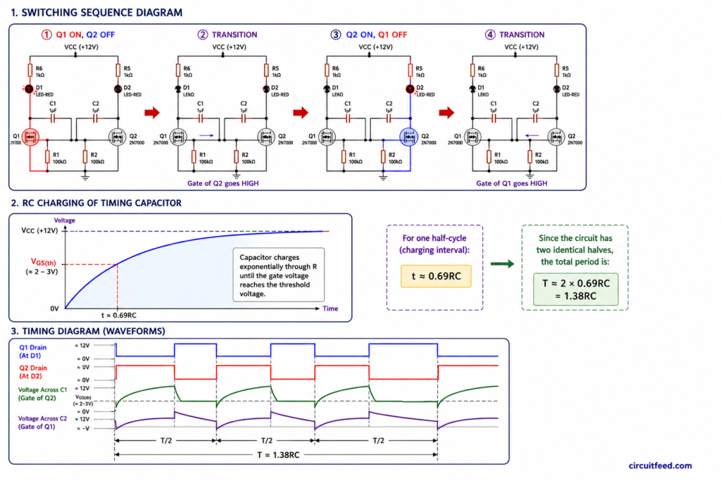
This minute imbalance is all that is needed to start oscillation. Suppose Q1 begins conducting first. Its drain voltage immediately falls toward ground potential. Because capacitor C1 is connected between the drain of Q1 and the gate of Q2, this sudden voltage change is transferred directly to Q2’s gate as a negative-going pulse. The pulse forces Q2 firmly into the OFF state.
Meanwhile, capacitor C1 slowly charges through resistor R2. As its voltage rises, the gate voltage of Q2 also increases. Eventually, the gate-to-source voltage reaches the threshold voltage of the MOSFET, allowing Q2 to switch ON. When this occurs, the entire sequence reverses. Q2 now pulls its drain voltage low, capacitor C2 transfers a negative pulse to the gate of Q1, and Q1 switches OFF. The circuit continuously alternates between these two stable conditions, producing complementary square waves indefinitely.
The Role of Positive Feedback
The rapid switching action is made possible by positive feedback. As soon as one MOSFET begins to conduct, it actively drives the opposite MOSFET toward cutoff. Rather than changing gradually, both transistors switch quickly between fully ON and fully OFF states. This regenerative behavior improves waveform quality, reduces transition time, and minimizes power dissipation inside the MOSFETs.
Positive feedback is one of the defining characteristics of every astable multivibrator. Without the cross-coupled capacitors providing this feedback path, the circuit would never oscillate.
Understanding the Timing Network
The oscillation frequency is determined entirely by the resistor-capacitor network. After each switching event, the timing capacitor charges exponentially through its associated resistor until the opposite MOSFET reaches its gate threshold voltage. The charging process follows the well-known RC exponential equation.
This exponential charging characteristic is responsible for the delay between switching events. Larger resistor or capacitor values increase the charging time and therefore reduce the output frequency, while smaller values produce faster oscillation.
In the next section, we will follow every switching event in chronological order, examine how each capacitor charges and discharges, derive the oscillation equations, calculate the output frequency mathematically, and explain why the well-known timing approximation of approximately 1.38RC accurately predicts the oscillation period of this circuit.
Step-by-Step Working Principle of the MOSFET Square Wave Generator
Although the circuit contains only two MOSFETs, two resistors, and two capacitors, the switching process is surprisingly elegant. The oscillator continuously alternates between two stable states. During one half-cycle, Q1 conducts while Q2 remains OFF. During the next half-cycle, the roles reverse. This continuous alternation produces two square-wave outputs that are equal in frequency but opposite in phase.
To fully understand the operation, it is helpful to examine each stage individually. Rather than thinking of both MOSFETs switching simultaneously, imagine the oscillator progressing through a sequence of events that repeat indefinitely.
Stage 1 – Initial Power-Up
Assume Q1 begins conducting slightly earlier than Q2.
Stage 2 – Q1 Turns ON
Since capacitor C1 is connected between the drain of Q1 and the gate of Q2, the sudden negative transition appears almost instantly at the gate of Q2.
The capacitor momentarily behaves as a short circuit for rapid voltage changes.
Consequently, the gate voltage of Q2 becomes negative with respect to its source.
Q2 is therefore driven even further into the OFF state.
Stage 3 – Capacitor C1 Begins Charging
After the initial switching event, capacitor C1 no longer behaves like a short circuit. Instead, it starts charging through resistor R2.
The charging current is very small because MOSFET gates draw almost no steady-state current.
This allows the capacitor to charge according to the classical exponential RC charging equation.
V_C(t)=V_{DD}\left(1-e^{-t/(RC)}\right)\\
V_{DD} = V_{CC} = +12V
As capacitor C1 charges, the gate voltage of Q2 rises gradually toward the supply voltage.
The charging process is not linear. Initially the voltage rises quickly, but as the capacitor approaches its final value the charging rate decreases exponentially.
Stage 4 – Q2 Reaches Threshold Voltage
Every enhancement-mode MOSFET begins conducting only after its gate-to-source voltage exceeds the threshold voltage.
For the 2N7000, the threshold voltage typically lies between 2 V and 4 V, depending on the individual device.
V_{GS}>V_{GS(th)}
Eventually the voltage across capacitor C1 becomes high enough that the gate of Q2 reaches this threshold level.
At this instant, Q2 begins to conduct.
Stage 5 – Regenerative Switching
As soon as Q2 switches ON, its drain voltage collapses rapidly toward ground.
Capacitor C2 immediately transfers this sudden voltage transition to the gate of Q1.
The gate voltage of Q1 therefore drops sharply below its previous value.
Q1 switches OFF almost instantaneously.
This positive feedback mechanism is called regenerative switching. Instead of changing slowly, both MOSFETs reinforce each other’s switching action and rapidly exchange states.
Stage 6 – The Process Repeats
Now capacitor C2 begins charging through resistor R1.
Its voltage increases exponentially until Q1 once again reaches its threshold voltage.
Q1 then turns ON, forcing Q2 OFF, and the complete sequence repeats indefinitely.
The oscillator therefore requires no external trigger or clock source.
Why Are the Outputs 180° Out of Phase?
Observe the drain terminals of both MOSFETs.
Whenever Q1 is ON, its drain voltage is approximately zero volts because current flows through the MOSFET channel.
At exactly the same moment, Q2 is OFF, so its drain is pulled upward by resistor R5 toward the positive supply.
Half a cycle later the situation reverses.
Consequently, the two drain voltages are logical inverses of each other.
| Operating State | Drain of Q1 | Drain of Q2 |
|---|---|---|
| Q1 ON, Q2 OFF | ≈0 V | ≈12 V |
| Q1 OFF, Q2 ON | ≈12 V | ≈0 V |
Because one output is always HIGH while the other is LOW, the phase difference between the two outputs is approximately 180 degrees.
Deriving the Oscillation Period
The oscillation frequency depends entirely on the time required for one timing capacitor to charge from its initial voltage until the opposite MOSFET reaches its threshold voltage.
For a symmetrical astable multivibrator where both resistors and both capacitors are identical, experimental analysis shows that the total oscillation period can be approximated by:
T \approx 1.38RC
The constant 1.38 is simply twice the natural logarithm of two.
Since
\ln(2)\approx0.693
the complete oscillation consists of two equal charging intervals.
T=2\times0.693RC\approx1.386RC
For practical engineering calculations, the value is rounded to 1.38RC.
Frequency Equation
Frequency is simply the reciprocal of the oscillation period.
f=\frac{1}{T}
Substituting the previous equation gives the well-known design formula.
f=\frac{1}{1.38RC}
This simple relationship makes the oscillator extremely easy to design. Doubling either the resistor or capacitor approximately halves the oscillation frequency, while reducing either value increases the output frequency.
Example Calculation
Using the component values shown in the schematic:
R=100\,k\Omega
C=1\,\mu F
The oscillation period becomes:
T=1.38\times100000\times1\times10^{-6}=0.138\,s
The corresponding frequency is:
f=\frac{1}{0.138}\approx7.25\,Hz
Each LED therefore flashes approximately seven times per second while the drain outputs produce two clean complementary square waves.
Understanding the MOSFET Operating Regions During Oscillation
Many beginners imagine that both MOSFETs operate like variable resistors throughout the oscillation cycle. In reality, this circuit is designed so that each MOSFET spends almost all of its time in either the fully OFF state or the fully ON state. Only during the brief switching interval does the transistor pass through its linear operating region.
This switching behavior is one of the major advantages of using MOSFETs in oscillator circuits. Since power dissipation is highest when both voltage and current are present simultaneously, keeping the transition time as short as possible greatly improves efficiency.
During one half-cycle, Q1 is fully enhanced while Q2 is completely cut off. During the next half-cycle, the roles reverse. The circuit therefore behaves more like a digital flip-flop than a linear amplifier.
Cut-Off Region
When the gate voltage is below the threshold voltage, no conductive channel exists between the drain and source terminals. The MOSFET behaves almost like an open switch.
V_{GS}<V_{GS(th)}
In this region, the drain current is essentially zero.
I_D\approx0
Since almost no current flows through the drain resistor, the drain voltage rises close to the supply voltage VDD equal to 12V.
Enhancement Region
As the timing capacitor charges, the gate voltage gradually increases. Once the gate-to-source voltage exceeds the threshold voltage, a conductive channel begins to form inside the MOSFET.
V_{GS}>V_{GS(th)}
The drain current now increases rapidly and the drain voltage begins to fall. This falling drain voltage is immediately coupled to the opposite MOSFET through the timing capacitor, initiating regenerative switching.
Fully ON State
Once the MOSFET is fully enhanced, its drain-to-source resistance becomes very small compared to the 1 kΩ drain resistor. Consequently, almost the entire supply voltage appears across the resistor and LED while the MOSFET itself drops only a small voltage.
V_{DS}\approx0
This produces a clean logic LOW level at the drain output.
Why the Gate Draws Almost No Current
One of the most important characteristics of a MOSFET is its insulated gate structure. Unlike a bipolar transistor, whose base requires continuous current, the MOSFET gate is electrically isolated by an extremely thin layer of silicon dioxide.
Because of this insulation, the steady-state gate current is practically zero.
I_G\approx0
The timing capacitor therefore charges almost entirely through the resistor without significant loading from the MOSFET gate. This is why RC timing with MOSFETs is usually more predictable than with bipolar transistor oscillators.
Current Flow During Each Half-Cycle
Understanding the current path helps explain why the oscillator continues indefinitely.
Assume Q1 is conducting.
The load current follows this path:
+12 V → R6 → LED D1 → Drain of Q1 → Source of Q1 → Ground
At the same time, capacitor C1 slowly charges through resistor R2 until Q2 reaches its switching threshold.
Once Q2 turns ON, the entire current path transfers to the opposite side of the circuit.
Only one LED receives current at any instant, which explains why the LEDs blink alternately.
How Positive Feedback Produces Fast Switching
The oscillator would not function correctly without positive feedback.
Suppose Q2 begins to turn ON.
Its drain voltage immediately decreases.
This voltage transition passes through capacitor C2 and pulls the gate voltage of Q1 downward.
As Q1 begins turning OFF, its drain voltage rises sharply.
Capacitor C1 transfers this rising voltage back to the gate of Q2, forcing Q2 further into conduction.
Each transistor therefore reinforces the switching action of the other.
This regenerative process produces nearly vertical output transitions even though the capacitor charging process itself is relatively slow.
Effect of Component Tolerances
No two electronic components are perfectly identical. Every resistor, capacitor, and MOSFET is manufactured with a tolerance that causes slight variations in electrical characteristics.
Typical tolerances include:
- Resistors: ±1% to ±5%
- Electrolytic capacitors: ±10% to ±20%
- 2N7000 threshold voltage: approximately 2 V to 4 V
These tolerances slightly affect oscillation frequency and duty cycle. Two circuits built with identical nominal values may therefore oscillate at slightly different frequencies.
This behavior is completely normal and should not be mistaken for a design error.
Frequency Accuracy
The theoretical frequency equation assumes ideal components and identical MOSFET characteristics.
In practice, the actual oscillation frequency depends on several additional factors:
- Capacitor tolerance
- Resistor tolerance
- MOSFET threshold voltage variation
- Gate capacitance
- VDD to GND voltage difference
- Temperature
Consequently, the measured frequency may differ from the calculated value by several percent. For most LED flashers, clock indicators, and demonstration circuits, this variation is insignificant. However, if precise timing is required, precision resistors, film capacitors, or crystal-controlled oscillators should be considered.
How to Change the Oscillation Frequency
The oscillation frequency is determined solely by the RC timing network.
f=\frac{1}{1.38RC}
This equation immediately shows how component values influence frequency.
| Modification | Result |
|---|---|
| Increase R | Frequency decreases |
| Decrease R | Frequency increases |
| Increase C | Frequency decreases |
| Decrease C | Frequency increases |
For example, replacing the 1 µF capacitors with 100 nF capacitors increases the frequency by approximately ten times. Likewise, replacing the 100 kΩ resistors with 1 MΩ resistors reduces the frequency by approximately a factor of ten.
Selecting Suitable Component Values
The component values shown in the schematic provide a slow oscillation of approximately 7 Hz, making the alternating LED flashes easy to observe. For audio-frequency oscillators or digital clock generators, the resistor and capacitor values can be reduced accordingly.
| R | C | Approximate Frequency |
|---|---|---|
| 100 kΩ | 1 µF | 7.25 Hz |
| 47 kΩ | 100 nF | 154 Hz |
| 10 kΩ | 100 nF | 724 Hz |
| 10 kΩ | 10 nF | 7.24 kHz |
This wide operating range makes the circuit useful for everything from slow LED blinkers to low-frequency pulse generators and logic experiments.
In the next part, we will examine practical design improvements, PCB layout recommendations, suitable MOSFET alternatives, simulation tips, troubleshooting methods, common mistakes, and real-world applications. These engineering considerations will help transform this simple educational circuit into a reliable design for practical projects.



Leave a Reply