
If you have ever opened a microcontroller datasheet, studied an electronic schematic, or connected an Arduino sensor module, you have almost certainly encountered labels such as VCC, VDD, VSS, and GND. At first glance these names appear to describe exactly the same thing—a power supply and a ground connection. However, they originated from different generations of semiconductor technology and still carry important engineering meaning today.
One integrated circuit may label its positive supply pin as VCC, while another identical-looking device uses VDD. A CMOS microcontroller often contains pins marked VDD and VSS, whereas an operational amplifier may use V+ and V−. Modern development boards frequently combine all of these names on the same PCB. Without understanding their history, it is easy to assume that manufacturers simply choose different labels at random. In reality, every name has a historical and technological origin that reflects the evolution of electronic devices over the last seventy years.
This guide goes far beyond the short definitions commonly found online. Instead of merely stating that “VCC is collector voltage” or “VDD is drain voltage,” we will explore why these names were created, how semiconductor technology shaped their evolution, and why engineers continue using them even though today’s integrated circuits are vastly different from the discrete transistors that introduced these conventions.
Understanding power rail names is not about memorizing abbreviations. It is about understanding the historical evolution of electronic engineering itself.
Why Do Power Supply Pins Have Different Names?
This is one of the most frequently misunderstood topics in electronics. Beginners often ask questions such as:
- Why do Arduino modules use VCC?
- Why do STM32 microcontrollers use VDD?
- Is VSS always ground?
- Why does one datasheet show GND while another shows VSS?
- Can VCC and VDD be connected together?
- Why are there separate analog and digital ground pins?
Although these questions appear unrelated, they all originate from a single concept: electrical naming conventions developed alongside semiconductor technology. Every generation of electronic devices introduced its own terminology, and many of those conventions remain in use today because engineers, manufacturers, textbooks, and industry standards have continued to adopt them.
To fully understand VCC, VDD, VSS, and GND, we must first travel back to the early days of electronic engineering—long before integrated circuits, microcontrollers, or MOSFETs existed.
The Evolution of Power Rail Names
The terminology used on modern circuit diagrams did not appear overnight. It evolved over several decades as electronic technology progressed through multiple generations of devices. Each generation introduced new active components, and with them came new naming conventions for supply rails.
| Era | Dominant Device | Typical Supply Naming |
|---|---|---|
| 1900–1950 | Vacuum Tubes | B+, B−, Heater Supply |
| 1950–1975 | Bipolar Junction Transistors (BJTs) | VCC, VEE |
| 1970–Present | MOSFETs and CMOS | VDD, VSS |
| Modern Embedded Systems | Mixed Technologies | VCC, VDD, GND, AVDD, DVDD, AGND, DGND and many others |
Notice that modern electronic systems often combine terminology from every historical period. A single embedded development board may contain a CMOS microcontroller powered through VDD, a USB connector supplying VBUS, a switching regulator with VIN and VOUT, analog circuitry referenced to AGND, and sensor connectors labelled simply as VCC and GND.
This mixture of names is not incorrect—it reflects the remarkable evolution of electronics rather than inconsistency.
Before Transistors: The Vacuum Tube Era
Long before the invention of the transistor, electronic equipment relied on thermionic vacuum tubes. Radios, military communication systems, laboratory instruments, and early computers all used vacuum tubes as amplifiers and switches.
Unlike semiconductor devices, vacuum tubes required multiple supply voltages. A low-voltage heater warmed the cathode, while a much higher DC voltage powered the anode (also called the plate). Engineers referred to this positive high-voltage rail as B+, while the return rail became known as B−.
These labels had nothing to do with collectors, drains, or semiconductor junctions because none of those devices had been invented yet. Instead, they originated from battery designations commonly used in early radio equipment. Separate batteries powered the filament, bias network, and plate supply, leading to familiar terms such as A battery, B battery, and C battery.
Although modern electronic circuits no longer use these names, the concept of assigning meaningful labels to different power rails began during this period and established a convention that continues to influence electrical engineering today.
The Transistor Revolution Changed Everything
The invention of the bipolar junction transistor (BJT) during the late 1940s fundamentally changed electronic circuit design. Vacuum tubes gradually disappeared from commercial equipment, replaced by smaller, cooler, more reliable semiconductor devices.
Unlike vacuum tubes, a bipolar transistor contains three terminals:
- Collector (C)
- Base (B)
- Emitter (E)
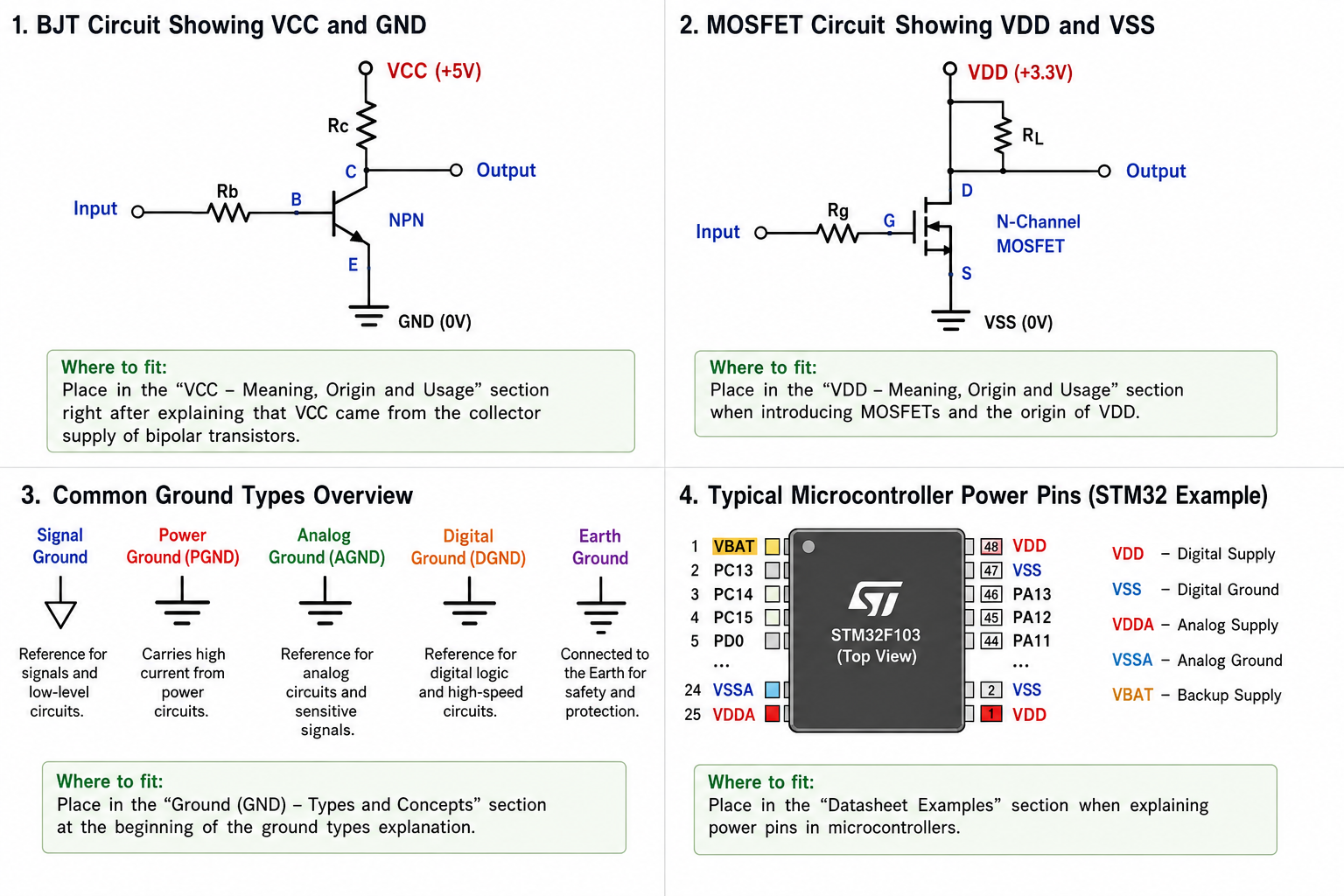
Since the collector was normally connected to the positive supply rail in NPN transistor circuits, engineers naturally began referring to that supply as Collector Voltage, abbreviated VCC. Likewise, circuits that used a negative supply connected to emitters adopted the name VEE.
It is important to recognize that VCC originally described the supply rail associated with the collector terminal—not merely any positive voltage. Over time, however, the term became deeply established in engineering literature and gradually evolved into a generic name for the positive power supply in countless electronic circuits.
One of the most common misconceptions is that VCC always connects directly to a transistor collector. Historically this was true, but modern electronics uses the term much more broadly.
Today, countless integrated circuits labelled VCC contain no discrete collector terminals whatsoever. Nevertheless, decades of engineering practice have preserved the name because it remains instantly recognizable to designers around the world.
The MOSFET Revolution Introduced VDD and VSS
As semiconductor technology matured during the late 1960s and 1970s, engineers began moving away from bipolar transistor circuits toward another revolutionary device: the Metal-Oxide-Semiconductor Field-Effect Transistor (MOSFET). This transition was not simply an improvement in transistor performance; it fundamentally changed the architecture of integrated circuits. The change also introduced a new family of power supply names that are now familiar to every embedded systems engineer.
Unlike a bipolar transistor, which controls current flowing through a collector-emitter junction, a MOSFET controls conduction between two terminals called the Drain and the Source. Since these terminals replaced the collector and emitter in MOS technology, engineers naturally adopted new names for the power rails connected to them.
| Technology | Positive Supply | Reference Supply | Terminal Names |
|---|---|---|---|
| BJT | VCC | VEE | Collector – Base – Emitter |
| MOSFET | VDD | VSS | Drain – Gate – Source |
This historical relationship explains why the letters themselves appear different. The first letter V represents voltage, while the second letter identifies the transistor terminal that was traditionally connected to that supply rail. Therefore, VCC originally referred to the collector supply, whereas VDD referred to the drain supply.
Many introductory tutorials stop here, leaving readers with the impression that the story is complete. However, modern integrated circuits rarely contain only one type of transistor. Today’s microcontrollers, processors, memory chips, communication interfaces and analog devices integrate millions or even billions of MOSFETs together with other semiconductor structures. Consequently, the original meaning of VDD has evolved beyond a simple “drain voltage.”
Why Modern ICs Still Use Historical Names
A common question among engineering students is why manufacturers continue using names such as VCC and VDD when today’s integrated circuits no longer resemble the simple transistor circuits from which those names originated. The answer lies in one of the most important principles of engineering documentation: consistency across generations of technology.
Electronic components often remain in production for decades. Development tools, textbooks, university courses, military standards and industrial documentation all rely on established terminology. Renaming every supply pin each time semiconductor technology evolves would create unnecessary confusion and significantly complicate the interpretation of schematics and datasheets.
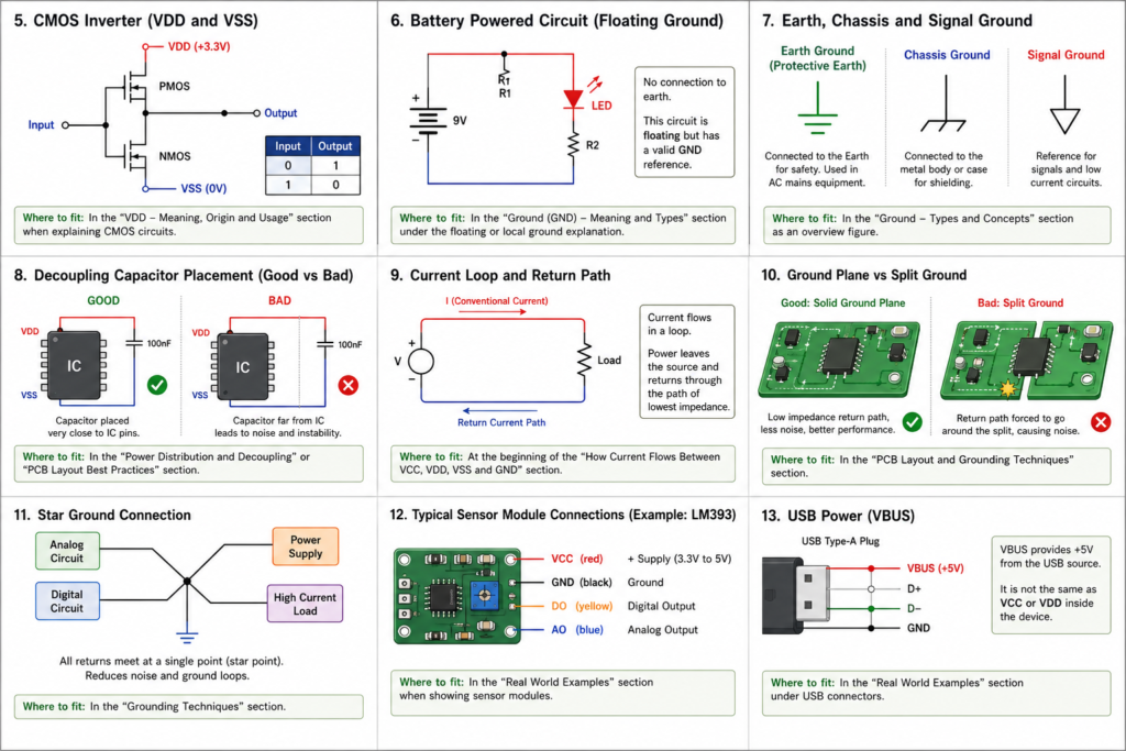
For this reason, engineers treat names such as VCC and VDD as engineering conventions rather than strict descriptions of transistor connections. The labels preserve historical continuity while providing designers with instantly recognizable power rail identifiers.
Today, VCC and VDD should be viewed primarily as naming conventions rather than literal collector or drain voltages. Their historical origins remain important, but their practical meaning has expanded with modern semiconductor technology.
The Rise of CMOS Technology
The widespread adoption of Complementary Metal-Oxide-Semiconductor (CMOS) technology accelerated the popularity of VDD and VSS. CMOS logic combines both NMOS and PMOS transistors on a single silicon substrate, allowing circuits to achieve extremely low static power consumption while maintaining high switching speeds.
Because CMOS circuits are built around MOSFET structures, manufacturers naturally continued using the MOS terminology introduced decades earlier. Consequently, nearly every modern microcontroller family—including STM32, ESP32, RP2040, many ARM Cortex-M devices and numerous digital ASICs—labels its primary power pins as VDD and VSS.
Interestingly, this convention remains in use even though the internal circuitry of these devices includes much more than simple MOS transistors. Voltage regulators, analog amplifiers, protection circuits, oscillators, memory arrays and communication peripherals all coexist on the same silicon die. Nevertheless, the external supply pins continue to follow the traditional CMOS naming convention.
Why Do Some CMOS Devices Still Use VCC?
At this point another question naturally arises. If CMOS technology introduced VDD and VSS, why do many CMOS integrated circuits still have pins labelled VCC and GND?
The answer is surprisingly simple. Semiconductor manufacturers are not obligated to follow a universal naming standard. Instead, each company generally maintains naming conventions that remain consistent across its own product families. Some manufacturers historically adopted bipolar terminology and retained it even after transitioning to CMOS manufacturing, while others fully embraced MOS terminology.
This explains why two functionally identical integrated circuits from different manufacturers may use completely different supply labels despite operating from the same voltage. One datasheet may specify VCC, while another specifies VDD, even though electrically both pins connect to the positive supply rail.
For an engineer reading a schematic, the important consideration is not the letters themselves but the function of the pin within the circuit. The datasheet always defines the required operating voltage, absolute maximum ratings and recommended connections regardless of the naming convention used.
Why Arduino Uses VCC but STM32 Uses VDD
This difference often confuses beginners because Arduino-compatible sensor modules typically provide pins labelled VCC and GND, whereas many STM32 development boards use VDD and VSS. Seeing both conventions on the same workbench leads many people to believe they represent incompatible power supplies.
In reality, both naming systems frequently describe exactly the same electrical connection. A 3.3 V power rail remains 3.3 V whether it is called VCC or VDD. Likewise, the reference node may be labelled GND or VSS depending on the design philosophy adopted by the manufacturer.
For example, an STM32 microcontroller may specify its operating supply as VDD = 3.3 V, while an external sensor module intended to interface with the same microcontroller provides a pin labelled VCC. Connecting the sensor’s VCC pin to the microcontroller’s 3.3 V VDD rail is completely correct because both names refer to the same positive supply potential in that application.
The electrical function determines compatibility—not the name printed beside the pin.
A Common Engineering Mistake
One of the most widespread misconceptions found in online tutorials is the statement that “VCC and VDD are exactly the same” or “VSS is always identical to GND.” While these simplifications may be acceptable for very basic circuits, they become misleading when designing precision analog systems, isolated power supplies, industrial controllers or high-speed digital hardware.
In many practical systems, VSS is connected directly to ground and VDD serves as the positive supply. However, there are equally important situations where VSS represents a floating reference node, an isolated return path or a local substrate reference rather than true earth or chassis ground. Understanding these distinctions becomes essential in mixed-signal PCB design, medical electronics, automotive systems and high-power converters.
In the next section, we will examine each power rail individually—beginning with VCC—before exploring how these names relate to modern concepts such as analog ground, digital ground, power ground, earth ground and isolated reference systems.
Understanding VCC — More Than Just a Positive Supply Voltage
Among all power rail names used in electronics, VCC is probably the most widely recognized. Even people with only a basic understanding of electronics associate VCC with the positive supply terminal of a circuit. While this interpretation is usually correct, it represents only the modern usage of the term. The original meaning of VCC is rooted in bipolar transistor technology, and understanding that history provides valuable insight into why the name continues to appear in countless schematics, datasheets, and development boards.
The abbreviation VCC literally means Voltage at the Common Collector or, more practically, the voltage supplied to the collector terminals of bipolar transistors. During the 1950s and 1960s, most electronic circuits were built using discrete NPN and PNP transistors. In a typical NPN amplifier or switching circuit, the collector was connected to the positive supply rail through a resistor or directly through the load. Since many collectors shared the same positive supply line, engineers began referring to that node as the common collector supply, eventually abbreviated as VCC.
The name therefore described the physical structure of the circuit rather than the voltage itself. This distinction is important because it explains why the abbreviation uses the letter C instead of simply indicating a positive voltage source.
Why the Letter “C”?
Electronic engineers often use terminal names as references for supply rails. In bipolar transistor circuits, the three terminals are:
- Collector (C)
- Base (B)
- Emitter (E)
Because the collector commonly connects to the positive power supply in NPN transistor circuits, the positive rail naturally became associated with the collector terminal. Similarly, circuits using dual power supplies frequently referenced the emitter side as VEE, indicating the supply connected to the emitter terminals.
This naming convention became deeply embedded in engineering literature. Textbooks, laboratory manuals, military standards, and semiconductor manufacturers all adopted VCC, making it one of the earliest standardized power rail names in solid-state electronics.
Typical NPN Circuit Using VCC
A simple transistor switch illustrates the historical origin of VCC remarkably well. In this circuit, the collector receives power directly from the positive supply through the load resistor, while the emitter connects to the reference node.
          VCC
           │
          RL
           │
           C
         ┌────┐
Input ───┤ B  │
         │NPN │
         └────┘
           E
           │
          GND
Notice that the collector is physically connected toward the positive supply rail. This simple relationship gave birth to the term VCC. Thousands of amplifier circuits, relay drivers, oscillators and logic gates published during the early transistor era followed this arrangement, reinforcing the terminology across the electronics industry.
Why VCC Survived the End of the Bipolar Era
As integrated circuits became increasingly complex, the direct relationship between the collector terminal and the positive supply gradually disappeared. Many digital integrated circuits no longer exposed individual transistor terminals to the user, yet manufacturers continued printing VCC beside the supply pin.
This persistence may seem surprising, but it reflects one of engineering’s most valuable principles: maintaining compatibility with existing knowledge. Changing the terminology would have required rewriting decades of documentation, redesigning educational material, updating laboratory exercises, and retraining engineers already familiar with established conventions.
Consequently, VCC evolved from a transistor-specific label into a general-purpose name for the positive supply rail. Today, millions of engineers immediately recognize VCC regardless of whether the internal circuitry actually contains bipolar transistors.
Where You Will Still Find VCC Today
Despite the widespread adoption of CMOS technology, VCC remains extremely common throughout modern electronics. In many cases, the name is retained simply because it is familiar to designers and technicians working with embedded systems.
| Device or Circuit | Typical Positive Rail |
|---|---|
| Arduino sensor modules | VCC |
| Relay modules | VCC |
| LM393 comparator modules | VCC |
| TTL logic ICs | VCC |
| Many EEPROM and memory ICs | VCC |
| Numerous analog integrated circuits | VCC |
Interestingly, several of these devices are manufactured using CMOS fabrication processes rather than bipolar technology. Nevertheless, manufacturers continue using VCC because the name is already familiar to their target audience and remains compatible with decades of existing documentation.
Does VCC Always Mean +5 Volts?
Absolutely not. Another widespread misconception is that VCC automatically implies a 5 V supply. This belief probably originated from early TTL logic families, where +5 V operation was nearly universal. Modern electronic systems, however, operate over a wide range of supply voltages.
Depending on the application, a VCC rail may be:
- 1.2 V in modern processors
- 1.8 V in memory devices
- 3.3 V in embedded controllers
- 5 V in logic circuits
- 12 V in industrial control equipment
- 24 V in PLC systems
- 48 V in communication infrastructure
The name identifies the function of the rail rather than its voltage level. Always consult the device datasheet to determine the required operating voltage.
Can VCC Be Negative?
In conventional single-supply electronic circuits, VCC is almost always the most positive supply rail. However, voltage is always measured relative to a chosen reference point. In isolated power systems, floating converters, differential measurement equipment, or specialized laboratory setups, the absolute voltage of VCC depends entirely on the selected reference node.
For example, an isolated DC-DC converter may produce an output supply that is electrically floating with respect to earth ground. Inside that isolated system, the positive rail may still be called VCC even though neither terminal has a fixed potential relative to the outside world.
Voltage names describe relationships within a circuit, not absolute electrical potential with respect to the Earth.
Engineering Insight
Experienced engineers rarely rely solely on a supply rail’s name when interpreting a schematic. Instead, they examine the complete circuit topology, voltage ratings, component functions, and datasheet recommendations. Whether a designer chooses the label VCC, VDD, VIN, or simply +3.3 V, the electrical behavior is determined by the circuit itself rather than the text printed beside the wire.
This distinction becomes increasingly important when working with mixed-signal systems, isolated converters, precision instrumentation, or high-speed digital electronics, where several independent positive supply rails may coexist within a single design.
From VCC to VDD — Why the Industry Needed a New Naming Convention
By the late 1970s, semiconductor technology had entered a new era. MOSFETs and CMOS logic were rapidly replacing bipolar transistor circuits in digital electronics, leading to integrated circuits that no longer revolved around collector and emitter terminals. As a result, engineers required a naming convention that reflected the new device architecture without abandoning the structured terminology that had served the industry for decades. This transition gave rise to the now familiar pair: VDD and VSS.
Understanding VCC — More Than Just a Positive Supply Voltage
Among all power rail names used in electronics, VCC is probably the most widely recognized. Even people with only a basic understanding of electronics associate VCC with the positive supply terminal of a circuit. While this interpretation is usually correct, it represents only the modern usage of the term. The original meaning of VCC is rooted in bipolar transistor technology, and understanding that history provides valuable insight into why the name continues to appear in countless schematics, datasheets, and development boards.
The abbreviation VCC literally means Voltage at the Common Collector or, more practically, the voltage supplied to the collector terminals of bipolar transistors. During the 1950s and 1960s, most electronic circuits were built using discrete NPN and PNP transistors. In a typical NPN amplifier or switching circuit, the collector was connected to the positive supply rail through a resistor or directly through the load. Since many collectors shared the same positive supply line, engineers began referring to that node as the common collector supply, eventually abbreviated as VCC.
The name therefore described the physical structure of the circuit rather than the voltage itself. This distinction is important because it explains why the abbreviation uses the letter C instead of simply indicating a positive voltage source.
Why the Letter “C”?
Electronic engineers often use terminal names as references for supply rails. In bipolar transistor circuits, the three terminals are:
- Collector (C)
- Base (B)
- Emitter (E)
Because the collector commonly connects to the positive power supply in NPN transistor circuits, the positive rail naturally became associated with the collector terminal. Similarly, circuits using dual power supplies frequently referenced the emitter side as VEE, indicating the supply connected to the emitter terminals.
This naming convention became deeply embedded in engineering literature. Textbooks, laboratory manuals, military standards, and semiconductor manufacturers all adopted VCC, making it one of the earliest standardized power rail names in solid-state electronics.
Typical NPN Circuit Using VCC
A simple transistor switch illustrates the historical origin of VCC remarkably well. In this circuit, the collector receives power directly from the positive supply through the load resistor, while the emitter connects to the reference node.
          VCC
           │
          RL
           │
           C
         ┌────┐
Input ───┤ B  │
         │NPN │
         └────┘
           E
           │
          GND
Notice that the collector is physically connected toward the positive supply rail. This simple relationship gave birth to the term VCC. Thousands of amplifier circuits, relay drivers, oscillators and logic gates published during the early transistor era followed this arrangement, reinforcing the terminology across the electronics industry.
Why VCC Survived the End of the Bipolar Era
As integrated circuits became increasingly complex, the direct relationship between the collector terminal and the positive supply gradually disappeared. Many digital integrated circuits no longer exposed individual transistor terminals to the user, yet manufacturers continued printing VCC beside the supply pin.
This persistence may seem surprising, but it reflects one of engineering’s most valuable principles: maintaining compatibility with existing knowledge. Changing the terminology would have required rewriting decades of documentation, redesigning educational material, updating laboratory exercises, and retraining engineers already familiar with established conventions.
Consequently, VCC evolved from a transistor-specific label into a general-purpose name for the positive supply rail. Today, millions of engineers immediately recognize VCC regardless of whether the internal circuitry actually contains bipolar transistors.
Where You Will Still Find VCC Today
Despite the widespread adoption of CMOS technology, VCC remains extremely common throughout modern electronics. In many cases, the name is retained simply because it is familiar to designers and technicians working with embedded systems.
| Device or Circuit | Typical Positive Rail |
|---|---|
| Arduino sensor modules | VCC |
| Relay modules | VCC |
| LM393 comparator modules | VCC |
| TTL logic ICs | VCC |
| Many EEPROM and memory ICs | VCC |
| Numerous analog integrated circuits | VCC |
Interestingly, several of these devices are manufactured using CMOS fabrication processes rather than bipolar technology. Nevertheless, manufacturers continue using VCC because the name is already familiar to their target audience and remains compatible with decades of existing documentation.
Does VCC Always Mean +5 Volts?
Absolutely not. Another widespread misconception is that VCC automatically implies a 5 V supply. This belief probably originated from early TTL logic families, where +5 V operation was nearly universal. Modern electronic systems, however, operate over a wide range of supply voltages.
Depending on the application, a VCC rail may be:
- 1.2 V in modern processors
- 1.8 V in memory devices
- 3.3 V in embedded controllers
- 5 V in logic circuits
- 12 V in industrial control equipment
- 24 V in PLC systems
- 48 V in communication infrastructure
The name identifies the function of the rail rather than its voltage level. Always consult the device datasheet to determine the required operating voltage.
Can VCC Be Negative?
In conventional single-supply electronic circuits, VCC is almost always the most positive supply rail. However, voltage is always measured relative to a chosen reference point. In isolated power systems, floating converters, differential measurement equipment, or specialized laboratory setups, the absolute voltage of VCC depends entirely on the selected reference node.
For example, an isolated DC-DC converter may produce an output supply that is electrically floating with respect to earth ground. Inside that isolated system, the positive rail may still be called VCC even though neither terminal has a fixed potential relative to the outside world.
Voltage names describe relationships within a circuit, not absolute electrical potential with respect to the Earth.
Engineering Insight
Experienced engineers rarely rely solely on a supply rail’s name when interpreting a schematic. Instead, they examine the complete circuit topology, voltage ratings, component functions, and datasheet recommendations. Whether a designer chooses the label VCC, VDD, VIN, or simply +3.3 V, the electrical behavior is determined by the circuit itself rather than the text printed beside the wire.
This distinction becomes increasingly important when working with mixed-signal systems, isolated converters, precision instrumentation, or high-speed digital electronics, where several independent positive supply rails may coexist within a single design.
From VCC to VDD — Why the Industry Needed a New Naming Convention
By the late 1970s, semiconductor technology had entered a new era. MOSFETs and CMOS logic were rapidly replacing bipolar transistor circuits in digital electronics, leading to integrated circuits that no longer revolved around collector and emitter terminals. As a result, engineers required a naming convention that reflected the new device architecture without abandoning the structured terminology that had served the industry for decades. This transition gave rise to the now familiar pair: VDD and VSS.
Understanding VSS — The Most Misunderstood Power Rail in Electronics
After learning the historical development of VCC and VDD, it is tempting to assume that VSS simply represents “ground.” This explanation appears in countless tutorials, forum posts, and even educational videos. Although this simplification works for many beginner circuits, it is technically incomplete and becomes increasingly inaccurate as electronic systems become more sophisticated.
In modern engineering, one of the most common design mistakes is assuming that every pin labelled VSS is permanently connected to earth ground or that it can always be treated as an ordinary GND connection. Professional engineers know that the truth is more nuanced. VSS often serves as the reference node for a particular voltage domain, but that reference does not necessarily correspond to the global ground of the entire system.
Understanding this distinction is essential when working with mixed-signal electronics, isolated power supplies, battery-operated equipment, medical devices, industrial automation, communication interfaces and high-speed digital systems.
What Does VSS Actually Mean?
The abbreviation VSS originated from MOS transistor terminology in the same way that VDD originated from the drain terminal. In MOS technology, the source terminal commonly serves as the lower potential reference within a circuit. Consequently, engineers introduced the name VSS to represent the voltage associated with the common source connection.
Historically, the relationship was straightforward:
- VDD → Drain supply
- VSS → Source reference
As CMOS technology evolved, these names gradually became standardized across semiconductor manufacturers. Today, most CMOS integrated circuits continue using VDD and VSS regardless of their internal transistor complexity.
Why VSS Is Often Connected to Ground
In the majority of low-voltage digital systems, the source reference of NMOS transistors is connected to the circuit’s reference potential. Because this reference node is usually designated as ground, VSS and GND become electrically identical.
This is exactly what happens in many familiar electronic products:
- STM32 development boards
- ESP32 modules
- Raspberry Pi boards
- Arduino-compatible CMOS peripherals
- Digital sensors
- Flash memory ICs
When measuring these circuits with a multimeter, the VSS pin normally shows zero volts relative to the board’s ground plane. This observation explains why many educational resources simply state that VSS equals ground.
For simple circuits, this explanation is acceptable. For advanced engineering, however, it is incomplete.
The Hidden Assumption Most Tutorials Never Mention
Nearly every introductory electronics article assumes that an entire circuit operates from a single power supply with one common reference node. Under these conditions, VSS, GND and the negative terminal of the supply all become the same electrical point.
Modern electronic systems rarely satisfy this assumption.
A contemporary embedded controller may simultaneously contain:
- multiple voltage regulators,
- isolated communication interfaces,
- analog measurement circuitry,
- digital processors,
- USB interfaces,
- switch-mode power supplies,
- battery backup domains.
Each subsystem may establish its own local voltage reference. Consequently, the label VSS no longer guarantees that every point marked VSS throughout the product is electrically identical.
VSS identifies the reference node of a voltage domain. Whether that node is identical to the system ground depends entirely on the circuit architecture.
A Practical Example Using an Isolated Power Supply
Consider an industrial control system containing an isolated DC-DC converter. The converter creates an entirely new voltage domain that has no direct electrical connection to the primary power supply.
Primary Supply

+24 V
 │
 │
DC-DC Converter
 │
 ├────────── +5 V (VDD)
 │
 └────────── VSS

(Isolated Domain)

No direct connection
to chassis ground
or earth ground.
Inside this isolated domain, every digital integrated circuit may correctly identify its reference pin as VSS. Nevertheless, that VSS node is floating with respect to the primary power system. Connecting it directly to another ground without understanding the isolation barrier may defeat the intended design or even damage the equipment.
This example illustrates why experienced engineers interpret supply labels within the context of the complete circuit rather than relying solely on their names.
Multiple VSS Pins on the Same Integrated Circuit
As integrated circuits became increasingly complex, manufacturers began separating different functional blocks to improve electrical performance. It is now common to encounter devices with multiple VSS pins distributed around the package.
These additional reference pins reduce parasitic inductance, lower voltage drops caused by switching currents, improve electromagnetic compatibility and provide cleaner return paths for high-speed signals.
Although several pins may all carry the name VSS, they usually connect together internally or are intended to be joined externally using a low-impedance ground plane according to the manufacturer’s PCB layout recommendations.
Why Analog and Digital Circuits Sometimes Use Different Reference Pins
Many modern microcontrollers contain precision analog peripherals such as analog-to-digital converters, digital-to-analog converters, operational amplifiers and voltage references. These circuits are extremely sensitive to electrical noise generated by the high-speed switching activity of the processor core.
To minimize interference, manufacturers often provide separate reference pins such as:
- VSSA (Analog Source Supply Reference)
- VSSD (Digital Source Supply Reference)
- AGND (Analog Ground)
- DGND (Digital Ground)
These labels do not imply completely isolated systems. Instead, they encourage PCB designers to control the return current paths so that noisy digital switching currents do not flow through sensitive analog measurement circuits.
We will study analog ground and digital ground in detail later because they represent one of the most misunderstood subjects in PCB design.
Common Misconceptions About VSS
| Common Statement | Engineering Reality |
|---|---|
| VSS always means ground. | Only if the circuit defines VSS as its ground reference. |
| Every VSS pin is connected to Earth. | Most electronic products are isolated from Earth. |
| VSS is always 0 volts. | Voltage depends on the chosen reference node. |
| VSS and negative supply are identical. | Not necessarily in dual-supply or floating systems. |
| Every VSS pin can be connected anywhere. | Always follow the manufacturer’s PCB layout recommendations. |
VSS Is a Reference—Not a Universal Ground
The most important concept to remember is that VSS defines the reference potential for a particular circuit or voltage domain. In many practical electronic designs that reference coincides with the system ground, which is why beginners often encounter the simplified explanation that “VSS equals ground.” However, professional circuit designers understand that this relationship exists because of the circuit implementation—not because the abbreviation itself requires it.
This distinction becomes even more important when we examine the term GND. Unlike VCC, VDD and VSS, the label GND does not originate from transistor terminology. Instead, it represents a much broader electrical concept whose meaning changes depending on the type of system being designed. Understanding GND properly requires separating several concepts that are often incorrectly treated as identical, including signal ground, earth ground, chassis ground, protective earth, analog ground and digital ground.
What Is GND? Understanding the Most Important Reference in Electronics
Among all electrical symbols found on schematics, PCB layouts and electronic datasheets, GND (Ground) is undoubtedly the most frequently used. Almost every electronic circuit contains at least one ground symbol, and most beginners naturally assume that every ground symbol represents exactly the same electrical point. Surprisingly, this assumption is one of the largest sources of confusion in practical electronics.
Unlike VCC, VDD and VSS, which originated from semiconductor device terminology, the word Ground does not describe any transistor terminal. Instead, it represents an electrical reference point chosen by the circuit designer. Every voltage measurement, whether performed by a multimeter, oscilloscope or analog-to-digital converter, is always measured relative to some reference. In most electronic circuits, that reference is labelled GND.
This definition appears simple, but it leads to an important realization: Ground is not necessarily Earth. In fact, many electronic systems operate for their entire lifetime without ever being electrically connected to the Earth.
Ground is a reference potential selected by the circuit designer. Earth is a physical connection to the planet. These two concepts often coincide, but they are not the same thing.
Why Every Circuit Needs a Reference Point
Voltage is not an absolute quantity. It always describes the difference in electrical potential between two points. Saying that a wire carries “5 volts” is incomplete unless we specify five volts with respect to what?
Mathematically, voltage is defined as the potential difference between two nodes.
V_{AB}=V_A-V_B
Here, VB acts as the reference node. If we choose this node to represent zero volts, then every other voltage in the circuit is measured relative to it. This chosen reference node is what engineers normally call Ground (GND).
Notice something important. Nothing in this equation requires the reference point to be physically connected to the Earth. The reference exists simply because voltage measurements require one.
A Simple Battery Demonstrates the Concept Perfectly
Consider a small battery powering an LED. This is one of the simplest electrical systems imaginable.
      +9V
       │
      LED
       │
    Resistor
       │
Battery (-)
       │
      GND
In this circuit, engineers usually label the battery’s negative terminal as GND. Doing so establishes the voltage reference for the entire circuit. Consequently, the positive battery terminal measures approximately +9 V relative to GND.
However, this battery-powered circuit has absolutely no electrical connection to the Earth beneath your feet. If you hold the battery in your hand, the entire circuit simply “floats” electrically. Nevertheless, it still has a perfectly valid ground reference.
This example immediately disproves one of the most common misconceptions found in beginner electronics:
Ground does not require an Earth connection.
Then Why Is It Called Ground?
The term Ground originates from electrical power distribution systems, where one conductor is intentionally connected to the Earth to improve safety and stabilize system voltage. As electronics evolved, engineers adopted the same word to describe the common reference node inside circuits because it represented the “zero-volt” point for measurements.
Over time, these two meanings became intertwined. Today, engineers routinely use the word ground in two different contexts:
- The electrical reference node inside a circuit.
- A conductor physically connected to the Earth.
Although both are called ground, they are not automatically the same electrical point.
Different Types of Ground Used in Electronics
Professional electronic systems rarely contain just one kind of ground. Instead, engineers deliberately separate different return paths to improve safety, reduce electrical noise and enhance electromagnetic compatibility.
| Ground Type | Main Purpose |
|---|---|
| Signal Ground | Reference for electronic signals |
| Power Ground | High-current return path |
| Analog Ground (AGND) | Reference for precision analog circuits |
| Digital Ground (DGND) | Reference for digital logic |
| Chassis Ground | Connection to equipment enclosure |
| Protective Earth (PE) | Electrical safety |
| Frame Ground (FG) | Industrial equipment structure |
Although these grounds may eventually connect together at one carefully selected location, treating them as identical throughout an entire PCB often results in excessive electrical noise, unstable measurements and electromagnetic interference.
Ground Is Also the Return Path for Current
Perhaps the most overlooked concept in electronics education is that ground is not simply a voltage reference. It also forms the return path through which electrical current completes its journey back to the power source.
According to Kirchhoff’s Current Law, current leaving a source must eventually return to it.
\sum I = 0
Every milliampere delivered by a power supply eventually returns through some conductor. In many electronic systems, this conductor is the ground network or ground plane. Consequently, ground carries real electrical current rather than acting as an imaginary zero-volt line.
This insight has profound consequences for PCB design. If high-current switching signals share the same narrow return path as sensitive analog measurements, voltage drops develop along the ground conductor. Even milliohms of resistance can generate measurable noise.
V_{drop}=I\times R
Although this equation appears elementary, it explains countless practical problems encountered in real electronic products. A ground trace carrying several amperes may develop tens or hundreds of millivolts across its length. Sensitive ADC inputs referenced to that same conductor will interpret this voltage drop as measurement error.
Professional PCB designers think of ground as a current-carrying conductor—not simply as a zero-volt symbol drawn on a schematic.
Why Modern PCBs Use Large Ground Planes
Early electronic circuits often connected ground using individual wires or narrow PCB traces. As operating frequencies increased and integrated circuits became faster, engineers discovered that these narrow return paths introduced unwanted resistance, inductance and electromagnetic radiation.
Modern multilayer PCBs therefore dedicate entire copper layers to ground. These continuous ground planes provide several important advantages:
- Lower electrical resistance.
- Lower parasitic inductance.
- Reduced electromagnetic interference (EMI).
- Improved signal integrity.
- Better heat spreading.
- More predictable return current paths.
For this reason, experienced PCB designers rarely think of ground as merely “zero volts.” Instead, they view it as one of the most important conductors in the entire system.
Is GND the Same as VSS?
We can now answer one of the most frequently searched questions on the Internet with greater precision than the simplified explanations commonly found online.
In many low-voltage CMOS circuits, VSS is directly connected to GND, making both labels electrically identical. However, this equivalence exists because of the designer’s implementation rather than because the names themselves mean the same thing.
VSS originates from MOS transistor terminology and identifies the reference supply of a voltage domain. GND identifies the electrical reference chosen for measurements and current return. In many practical circuits these concepts overlap completely, but advanced systems containing isolated supplies, multiple voltage domains or mixed-signal architectures may intentionally distinguish between them.
The next section builds upon this foundation by examining Earth Ground, Chassis Ground, Signal Ground, Power Ground, Analog Ground and Digital Ground. Understanding how these grounds interact is essential for designing reliable electronic equipment and avoiding one of the most common causes of noise and measurement errors in modern PCB design.
Earth Ground, Chassis Ground, Signal Ground, Power Ground, AGND and DGND Explained
After understanding that GND is an electrical reference rather than automatically being the Earth itself, we can now explore one of the most important concepts in practical electronics. Professional electronic systems rarely contain a single type of ground. Instead, modern equipment intentionally separates different ground systems to improve electrical safety, reduce electromagnetic interference (EMI), increase measurement accuracy and ensure stable operation.
This is the point where many beginners become confused because the word ground is used to describe several completely different electrical functions. Although these grounds may eventually connect together somewhere within a system, they should never be considered interchangeable without understanding their specific purpose.
The word “Ground” describes a function, not a physical wire. Two conductors may both be called ground while serving entirely different engineering purposes.
1. Earth Ground (Protective Earth or PE)
Earth Ground, often abbreviated as PE (Protective Earth), is the only ground that has a direct physical connection to the Earth. It exists primarily for human safety rather than normal circuit operation.
Inside homes, factories and laboratories, the earth conductor is connected to grounding electrodes buried in the soil. Metal enclosures of electrical equipment are connected to this protective conductor so that, if an insulation failure causes a live conductor to touch the chassis, the fault current flows safely to earth instead of through a person touching the equipment.
Under normal operating conditions, ideally no current should continuously flow through the protective earth conductor. It exists as a safety mechanism rather than as the intended return path for electronic circuits.
| Earth Ground Characteristics | Description |
|---|---|
| Main Purpose | Electrical safety |
| Connected to Earth? | Yes |
| Carries normal operating current? | Ideally No |
| Used in battery-powered devices? | Usually No |
Many portable electronic devices, such as smartphones, handheld multimeters and battery-powered development boards, operate perfectly without any earth connection because they are electrically isolated from the mains supply.
2. Chassis Ground
Chassis Ground refers to the conductive metal enclosure surrounding electronic equipment. Its purpose is mechanical shielding, electromagnetic compatibility and safety.
In desktop computers, oscilloscopes, industrial control cabinets and laboratory instruments, the chassis often connects to Protective Earth. However, this is not always the case. Battery-powered equipment may have a floating chassis with no electrical connection to earth at all.
Experienced PCB designers carefully decide where signal ground connects to chassis ground. Connecting them indiscriminately may create unwanted ground loops and increase electromagnetic interference.
3. Signal Ground
Signal Ground serves as the voltage reference for electronic signals. Digital logic levels, analog sensor outputs, communication interfaces and measurement circuits all require a stable reference potential to ensure reliable operation.
Unlike Protective Earth, signal ground almost always carries operating current. Every signal transmitted through a conductor must eventually return through another conductor, and in many systems that return path is the signal ground network.
For example, when a UART interface transmits serial data from one microcontroller to another, both devices must share a common signal reference. Without a common signal ground, the receiver cannot accurately determine whether the incoming voltage represents a logical HIGH or LOW.
A voltage signal has meaning only when both devices agree on the same reference potential.
4. Power Ground (PGND)
Power Ground (PGND) is the return path for high-current sections of a circuit. Examples include switching regulators, motor drivers, battery chargers, inverters, power amplifiers and high-current MOSFET stages.
These circuits may carry currents ranging from several amperes to hundreds of amperes. Even a small resistance in the return path produces measurable voltage drops according to Ohm’s Law.
V=IR
Suppose a ground trace has a resistance of only 20 mΩ. If a switching regulator returns 8 A through that conductor, the voltage drop becomes:
V=8\times0.02=0.16\text{ V}
A voltage error of 160 mV may be insignificant for a motor driver but disastrous for a precision 12-bit analog-to-digital converter. This simple calculation explains why engineers frequently separate high-current power ground from sensitive signal ground.
5. Analog Ground (AGND)
Analog Ground (AGND) provides the reference potential for precision analog circuits such as operational amplifiers, voltage references, analog-to-digital converters (ADC), digital-to-analog converters (DAC) and sensor conditioning circuits.
Analog circuits often process signals measured in microvolts or millivolts. Consequently, even a few millivolts of noise introduced through the ground network can significantly degrade measurement accuracy.
For this reason, PCB designers attempt to keep high-current switching return paths away from analog reference conductors. Many mixed-signal integrated circuits therefore provide separate AGND pins to encourage cleaner PCB layout.
6. Digital Ground (DGND)
Digital Ground (DGND) serves digital logic circuits containing rapidly switching transistors. Every clock edge, memory access, processor instruction and communication interface generates transient switching currents that flow through the digital ground network.
Unlike analog circuits, digital logic generally tolerates relatively large amounts of electrical noise. However, the rapidly changing currents associated with digital switching generate electromagnetic interference that can easily couple into nearby analog circuitry if the PCB layout is not carefully designed.
This is one reason why many microcontrollers include separate AGND and DGND pins even though they eventually connect together internally or externally.
Should AGND and DGND Be Connected Together?
One of the oldest rules taught in PCB design was to split analog and digital grounds completely. Modern high-speed PCB design has shown that this advice is often oversimplified and, in some situations, even harmful.
Today’s best practice depends on the manufacturer’s layout recommendations, PCB layer stack-up and signal frequencies. In many mixed-signal designs, AGND and DGND are connected together using a continuous ground plane rather than physically separating the copper into isolated islands.
The objective is not to isolate the grounds themselves but to control where return currents flow. Return current always seeks the lowest impedance path rather than simply the shortest physical distance. Understanding this principle is far more important than blindly following outdated grounding rules.
Modern PCB design focuses on controlling return-current paths rather than merely separating ground symbols.
Comparing Different Ground Types
| Ground Type | Main Purpose | Carries Current | Connected to Earth? |
|---|---|---|---|
| Earth Ground (PE) | Safety | Normally No | Yes |
| Chassis Ground | Shielding & Safety | Sometimes | Sometimes |
| Signal Ground | Voltage Reference | Yes | Not Required |
| Power Ground | High Current Return | Yes | Not Required |
| Analog Ground | Precision Measurements | Yes | Not Required |
| Digital Ground | Logic Switching | Yes | Not Required |
The Fundamental Principle Behind Every Ground System
Although engineers use many different names for grounds, every ground system serves one or more of three fundamental purposes:
- Providing a stable voltage reference.
- Returning electrical current to its source.
- Improving safety and electromagnetic compatibility.
Recognizing which of these functions a particular ground performs is far more valuable than simply memorizing abbreviations. Once this principle becomes clear, supply labels such as VCC, VDD, VSS, GND, AGND and DGND become much easier to interpret across datasheets, schematics and PCB layouts.
Now that we have established the meaning of the major power rail names, the next chapter will compare them directly in practical engineering applications. Rather than discussing each abbreviation individually, we will examine how VCC, VDD, VSS and GND relate to one another inside real electronic products, microcontrollers, development boards and sensor modules. This comparison resolves many of the questions that frequently arise when reading datasheets or wiring embedded systems.
How to Read Power Rail Names in Electronic Datasheets
After understanding the historical origin of VCC, VDD, VSS and GND, the next challenge is interpreting these names in real engineering documents. Opening the datasheet of a modern microcontroller or integrated circuit often reveals several unfamiliar supply pins instead of a single positive supply and ground connection.
For example, a contemporary microcontroller may contain separate pins labelled VDD, VDDA, VSS, VSSA, VBAT, VREF+ and VREF−. To someone encountering these labels for the first time, the circuit may appear unnecessarily complicated. In reality, each power rail exists because a modern integrated circuit performs many different functions simultaneously.
Unlike early integrated circuits that contained only a few hundred transistors, modern microcontrollers integrate processors, memories, analog-to-digital converters, digital-to-analog converters, oscillators, communication peripherals, voltage regulators, clock generators and protection circuits on a single silicon die. Supplying every functional block from one common power pin would reduce performance and increase electrical noise.
A Typical Modern Microcontroller Power System
The simplified diagram below illustrates the philosophy adopted by many semiconductor manufacturers.
              +3.3 V

                │
       ┌────────┴────────┐
       │                 │
      VDD              VDDA
       │                 │
 Digital Logic     Analog Circuits
 CPU               ADC
 Flash             DAC
 RAM               Comparator
 GPIO              Voltage Reference
       │                 │
      VSS             VSSA
       └────────┬────────┘
                │
              Ground Plane
Although the analog and digital sections eventually share a common reference, separating their supply pins allows PCB designers to minimize switching noise reaching sensitive analog circuitry.
Why Do Manufacturers Provide Multiple VDD Pins?
One of the first observations made when reading a high-pin-count microcontroller datasheet is that several pins carry exactly the same name. It is common to see four, six or even ten pins labelled VDD, together with an equal number of VSS pins.
This is not redundancy. Multiple supply pins improve electrical performance in several important ways.
- Lower supply impedance.
- Reduced voltage drop inside the package.
- Lower parasitic inductance.
- Improved transient current delivery.
- Better EMC performance.
- Higher switching speed.
Every output driver, processor core and communication peripheral demands current that changes within nanoseconds. Distributing this current through several supply pins dramatically improves power integrity compared with relying on a single connection.
More VDD pins usually indicate higher performance—not unnecessary complexity.
Understanding VDDA and VSSA
Many STM32, NXP, Microchip and Renesas microcontrollers provide dedicated analog supply pins named VDDA and VSSA. The additional letter A simply identifies the analog subsystem.
| Pin | Purpose |
|---|---|
| VDD | Main digital supply |
| VSS | Digital reference |
| VDDA | Analog supply |
| VSSA | Analog reference |
| VBAT | Backup battery supply |
| VREF+ | ADC reference voltage |
| VREF− | ADC reference return |
Ignoring these distinctions may reduce ADC accuracy by introducing digital switching noise directly into precision analog measurements. Consequently, manufacturers often recommend separate filtering, ferrite beads or dedicated decoupling capacitors for analog supply rails.
Why Arduino Sensor Modules Still Use VCC
An interesting observation is that many Arduino-compatible sensor modules continue using the labels VCC and GND, even though the integrated circuits mounted on those modules may internally use VDD and VSS.
The reason is largely practical rather than technical. Arduino popularized the labels VCC and GND for hobbyists, educators and beginners. Sensor manufacturers therefore adopted the same terminology to improve compatibility and reduce confusion during wiring.
Internally, however, the sensor IC may still be powered from VDD and referenced to VSS exactly as described in its semiconductor datasheet. The PCB simply translates the manufacturer’s terminology into labels that are familiar to the target audience.
An Engineer Reads the Datasheet Differently
Professional circuit designers rarely ask whether a pin is called VCC or VDD. Instead, they ask more meaningful engineering questions:
- What voltage range does this supply require?
- Is this an analog or digital power domain?
- Does the manufacturer require separate filtering?
- Which decoupling capacitors should be placed beside the pin?
- Is this rail always powered, or only during specific operating modes?
- Does this supply require a particular power-up sequence?
These questions determine whether a circuit operates reliably. The label printed beside the pin is simply the starting point for understanding the designer’s intent.
Why Different Semiconductor Manufacturers Use Different Power Rail Names
One question that even experienced engineers occasionally ask is why two integrated circuits performing nearly the same function use completely different power supply names. An Arduino development board may expose pins labelled VCC and GND, while an STM32 development board uses VDD and VSS. A Xilinx FPGA introduces names such as VCCINT and VCCIO, whereas an ESP32 module may provide VDD3P3, VDDA and VSSA. To someone unfamiliar with semiconductor history, these differences appear inconsistent. In reality, they reflect decades of engineering evolution rather than disagreement between manufacturers.
Every semiconductor company develops products over many years, often inheriting documentation styles, design philosophies and naming conventions established long before current device families existed. Once thousands of engineers become familiar with a terminology, changing every datasheet would create unnecessary confusion and break continuity across product generations. Consequently, manufacturers usually preserve their traditional naming systems while adapting them to newer technologies.
Different Names, Same Electrical Function
It is important to understand that supply rail names are primarily engineering conventions. They help describe the intended purpose of a connection but do not define its operating voltage. Two devices may require exactly the same 3.3 V supply even though one labels the input pin VCC and the other labels it VDD.
Professional engineers therefore begin by reading the electrical specifications rather than focusing on the supply label itself. The recommended operating voltage, absolute maximum ratings, power-up requirements and decoupling recommendations always determine how a device should be connected.
Common Naming Conventions Used by Major Semiconductor Manufacturers
| Manufacturer | Common Power Rail Names | Typical Device Families |
|---|---|---|
| STMicroelectronics | VDD, VSS, VDDA, VSSA, VBAT | STM32 Microcontrollers |
| Microchip Technology | VDD, VSS, AVDD, AVSS | PIC Microcontrollers |
| Atmel (AVR) | VCC, AVCC, GND, AREF | ATmega and ATtiny Series |
| Texas Instruments | VCC, GND, AVCC, DVCC | Logic ICs, Analog ICs, Amplifiers |
| NXP Semiconductors | VDD, VSS, VDDA | Kinetis, LPC, i.MX |
| Espressif Systems | VDD3P3, VDDA, VSSA | ESP32 Family |
| AMD Xilinx | VCCINT, VCCAUX, VCCIO | FPGA Devices |
| Intel (Altera) | VCCINT, VCCIO, VCCA | FPGA Devices |
Although the names vary considerably, their engineering purpose remains remarkably similar. Manufacturers simply extend traditional terminology to distinguish different voltage domains within increasingly complex integrated circuits.
Why FPGA Devices Use VCCINT and VCCIO
Field Programmable Gate Arrays (FPGAs) provide an excellent example of modern supply rail naming. Instead of a single positive supply, an FPGA often operates from several independent voltage domains optimized for different functional blocks.
| Supply Rail | Purpose |
|---|---|
| VCCINT | Internal FPGA logic core |
| VCCIO | Input and Output banks |
| VCCAUX | Auxiliary analog circuitry |
| VREF | Reference voltage for I/O standards |
This approach allows different parts of the integrated circuit to operate at voltages best suited to their electrical requirements. For example, the FPGA core may operate at 0.9 V to reduce power consumption, while external input/output banks communicate using 1.8 V, 2.5 V or 3.3 V logic levels.
Why AVR Microcontrollers Use AVCC Instead of VDDA
The AVR family of microcontrollers provides another interesting example. Since these devices were originally developed using the long-established VCC naming convention, their analog power pin became known as AVCC rather than VDDA. Functionally, however, AVCC performs essentially the same role as VDDA in many ARM-based microcontrollers—it supplies the analog subsystem while helping isolate sensitive measurements from digital switching noise.
This illustrates an important engineering principle: identical functions do not always share identical names. Understanding the purpose of a supply rail is considerably more valuable than memorizing its abbreviation.
Experienced engineers interpret power rail names as documentation aids rather than strict electrical standards. The datasheet always takes precedence over naming convention.
The Future of Power Rail Naming
As semiconductor devices continue integrating additional functional blocks, supply rail names are becoming increasingly descriptive. Modern processors now include rails dedicated to processor cores, memory interfaces, radio-frequency circuits, graphics engines, high-speed transceivers, security modules and always-on power domains. Rather than replacing traditional names such as VCC and VDD, manufacturers typically extend them by adding meaningful suffixes that identify the subsystem they power.
Consequently, future engineers are likely to encounter an even wider variety of supply names. Fortunately, once the historical principles discussed in this guide are understood, interpreting these new labels becomes straightforward because they all follow the same underlying philosophy.
VCC vs VDD vs VSS vs GND – Complete Engineering Comparison
After exploring the historical evolution of power rail terminology, individual supply names, grounding concepts and manufacturer conventions, we can now compare the four most common electrical labels used in modern electronics. This comparison summarizes not only their historical origins but also their practical applications in contemporary circuit design.
One important point should be emphasized before examining the table. None of these names defines a specific voltage level. A rail labelled VCC may operate at 1.8 V, 3.3 V, 5 V or even 48 V depending on the equipment. Likewise, VDD, VSS and GND describe the function of a node within a circuit rather than prescribing an absolute electrical potential.
Engineering Comparison Table
| Parameter | VCC | VDD | VSS | GND |
|---|---|---|---|---|
| Historical Origin | Bipolar Junction Transistor era | MOSFET / CMOS era | MOSFET / CMOS era | General electrical engineering |
| Name Derived From | Collector terminal | Drain terminal | Source terminal | Ground reference |
| Usually Represents | Positive supply | Positive supply | Reference supply | Reference node |
| Associated Device | BJT | MOSFET | MOSFET | Entire electrical system |
| Modern Meaning | Main positive rail | Main positive rail | Reference rail | Voltage reference and return path |
| Common in TTL Logic | Yes | Rare | No | Yes |
| Common in CMOS | Sometimes | Very Common | Very Common | Very Common |
| Typical Microcontrollers | AVR | STM32, ESP32, PIC | STM32, ESP32, PIC | All |
| Arduino Usage | Very Common | Rare | Rare | Very Common |
| Typical FPGA Usage | VCCINT, VCCIO | Some Devices | Internal Reference | Board Ground |
| Normally Positive? | Yes | Yes | No | Reference |
| Normally 0 Volts? | No | No | Usually | Usually |
| Always Earth Connected? | No | No | No | No |
| Can Float? | Yes | Yes | Yes | Yes |
| Current Return Path | No | No | Often | Yes |
| Appears on PCB | Frequently | Frequently | Frequently | Almost Always |
| Datasheet Frequency | High | Very High | Very High | Very High |
| Related Analog Rails | AVCC | VDDA | VSSA | AGND |
| Related Digital Rails | DVCC | DVDD | DVSS | DGND |
| Main Engineering Role | Power Delivery | Power Delivery | Reference Supply | Reference + Current Return |
| Used for Safety? | No | No | No | Only if connected to Protective Earth |
| Can Exist Without Earth? | Yes | Yes | Yes | Yes |
| Most Common Beginner Confusion | Always 5V | Always 3.3V | Always Ground | Always Earth |
What This Comparison Actually Tells Us
The comparison above reveals an important engineering principle. Although VCC, VDD, VSS and GND often appear together on the same schematic, they describe different aspects of an electrical system. VCC and VDD primarily identify positive supply rails, whereas VSS identifies the reference supply associated with MOS technology. Ground, on the other hand, describes the reference node used for voltage measurement and current return throughout the circuit.
Because modern electronic systems combine multiple semiconductor technologies, it is perfectly normal for a single product to contain both VCC and VDD simultaneously. For example, a development board may receive power through a connector labelled VCC while its onboard microcontroller uses VDD internally and its analog subsystem operates from VDDA. None of these names contradict one another; they simply reflect different engineering conventions applied to different parts of the system.
Modern electronic products often contain several power naming conventions simultaneously. Understanding the function of each rail is far more important than memorizing its abbreviation.
How Engineers Identify an Unknown Power Pin
Suppose you encounter an unfamiliar integrated circuit whose pins are labelled only by abbreviations. Instead of guessing their meaning, experienced engineers follow a systematic approach.
- Read the recommended operating conditions table.
- Locate the pin description section.
- Identify the required operating voltage.
- Determine whether the pin belongs to an analog or digital power domain.
- Check whether separate filtering or decoupling is recommended.
- Review the reference application schematic.
- Follow the PCB layout recommendations provided by the manufacturer.
This approach eliminates ambiguity and ensures that the power system is implemented exactly as intended by the device manufacturer.
The Most Important Rule to Remember
If there is one concept worth remembering from this entire discussion, it is this:
Never connect electrical pins based only on their names. Connect them based on their electrical specifications.
A power rail labelled VCC may require 5 V, while another device using the same name may require only 1.8 V. Likewise, two VDD pins may belong to completely different voltage domains within the same integrated circuit. Reading the datasheet is therefore an essential part of every engineering design process.
1900
│
├── Vacuum Tubes
│ B+
│ B-
│
1950
│
├── BJT
│ VCC
│ VEE
│
1970
│
├── MOSFET
│ VDD
│ VSS
│
1990
│
├── CMOS
│ AVDD
│ DVDD
│
2000
│
├── ARM
│ VDDA
│ VSSA
│
2010
│
├── FPGA
│ VCCINT
│ VCCAUX
│
2020+
│
└── Multi-domain Power
VCORE
VIO
VSYS
VBAT
The Evolution of Power Rail Names: From Vacuum Tubes to Modern Processors
Electronic terminology evolves much more slowly than semiconductor technology. Although transistors have progressed from discrete germanium devices to highly integrated multi-billion transistor processors, many of the power supply names introduced decades ago remain in active use today. This continuity is one reason why engineers working with both vintage equipment and modern embedded systems still encounter familiar names such as VCC, VDD and GND.
Understanding the historical development of these names provides much deeper insight than simply memorizing their definitions. Instead of viewing VCC, VDD, VSS and GND as unrelated abbreviations, they become milestones in the evolution of electronic engineering.
1900–1950: The Vacuum Tube Era
Before the invention of semiconductor transistors, electronic equipment relied entirely on thermionic vacuum tubes. Radios, radar systems, oscilloscopes and the earliest digital computers all used vacuum tubes as amplifiers and switches.
Power supplies during this period were described differently from modern electronic circuits. Instead of VCC or VDD, engineers commonly used:
- B+ — High-voltage plate supply.
- B− — Plate return.
- A Supply — Filament or heater supply.
- C Supply — Grid bias voltage.
These names originated from the separate batteries used in early portable radio equipment. Each battery served a different function, and the naming convention reflected its purpose rather than its voltage.
The idea of assigning descriptive names to power rails existed long before the transistor was invented.
1950–1970: The Bipolar Transistor Revolution
The invention of the bipolar junction transistor completely changed electronic design. Circuits became smaller, consumed less power and required significantly lower operating voltages. As transistor amplifiers replaced vacuum tubes, engineers naturally adopted new terminology based on transistor terminals.
The collector became associated with the positive supply rail, giving rise to the abbreviation VCC. Likewise, the emitter side of many transistor circuits introduced the complementary term VEE.
Because bipolar transistors dominated electronics for nearly two decades, these names became deeply embedded in textbooks, university courses and industrial documentation.
1970–1990: MOSFET and CMOS Technology
The rapid adoption of MOS technology introduced an entirely different transistor structure. Instead of collectors and emitters, MOSFETs use drains and sources. Consequently, engineers adopted the names VDD and VSS to describe the primary supply rails.
This period also witnessed the emergence of CMOS logic, whose extremely low power consumption made it the dominant semiconductor technology for digital integrated circuits.
Manufacturers developing CMOS products naturally adopted VDD and VSS throughout their documentation. These names remain the preferred convention for many microcontrollers and digital integrated circuits today.
1990–2010: Mixed-Signal Integrated Circuits
As integrated circuits became more sophisticated, digital processors were combined with analog peripherals, communication interfaces and precision measurement circuits. A single supply rail could no longer satisfy every functional block without introducing unwanted electrical noise.
Manufacturers therefore expanded the traditional naming system by adding descriptive prefixes and suffixes.
| Power Rail | Purpose |
|---|---|
| AVDD | Analog supply voltage |
| DVDD | Digital supply voltage |
| AVCC | Analog collector supply |
| AGND | Analog ground |
| DGND | Digital ground |
| PGND | Power ground |
This period marked the beginning of multi-domain power distribution inside integrated circuits.
2010–Present: Multi-Domain Power Architecture
Today’s processors, FPGAs and system-on-chip (SoC) devices contain billions of transistors operating at multiple voltage levels simultaneously. Instead of one positive supply and one ground connection, modern integrated circuits frequently include ten or more independent power domains.
Typical examples include:
- VCORE
- VDDIO
- VCCINT
- VCCAUX
- VBAT
- VSYS
- VUSB
- VDDRAM
- VREF
- VRTC
Each rail powers a specific functional block within the integrated circuit. This architecture reduces power consumption, improves signal integrity and allows different subsystems to operate at their optimum voltages.
A Timeline of Power Rail Evolution
| Period | Dominant Technology | Common Supply Names |
|---|---|---|
| 1900–1950 | Vacuum Tubes | B+, B−, A Supply, C Supply |
| 1950–1970 | BJT | VCC, VEE |
| 1970–1990 | MOSFET, CMOS | VDD, VSS |
| 1990–2010 | Mixed-Signal ICs | AVDD, DVDD, AGND, DGND |
| 2010–Present | SoC, FPGA, Multi-Core Processors | VCORE, VDDIO, VCCINT, VBAT, VSYS and many others |
One remarkable aspect of this timeline is that none of the earlier naming conventions disappeared completely. Instead, every new generation inherited the previous terminology while extending it to describe increasingly complex semiconductor devices. As a result, engineers today routinely encounter VCC, VDD, VSS, GND, AVDD, DGND and many other supply names within the same electronic product.
Power rail names are not isolated abbreviations. They form a historical record of how electronic engineering evolved from vacuum tubes to modern integrated circuits.
Common Misconceptions About VCC, VDD, VSS and GND
Although VCC, VDD, VSS and GND have been used for decades, they remain among the most misunderstood abbreviations in electronics. Many misconceptions originate from simplified explanations intended for beginners. While these shortcuts may be adequate for introductory circuits, they often become misleading when designing professional electronic equipment.
The following sections explain some of the most common misconceptions encountered in engineering classrooms, online forums and practical circuit design.
Misconception 1: VCC Always Means +5 Volts
One of the oldest misconceptions in electronics is that VCC automatically indicates a 5 V supply. This idea became widespread because early TTL logic families almost exclusively operated from +5 V.
Modern electronics no longer follows this convention. A supply labelled VCC may be:
- 1.2 V inside a processor core
- 1.8 V in DDR memory
- 3.3 V in embedded systems
- 5 V in logic circuits
- 12 V in industrial electronics
- 24 V in PLC equipment
- 48 V in communication systems
The label identifies the function of the rail—not its voltage.
Misconception 2: VDD Always Means 3.3 Volts
Since many modern microcontrollers operate from 3.3 V, some engineers mistakenly associate VDD exclusively with this voltage. In reality, VDD simply identifies the primary positive supply for a MOS or CMOS device.
Depending on the integrated circuit, VDD may range from less than one volt inside advanced processors to more than twenty volts in specialized industrial devices.
Misconception 3: VSS Is Always Ground
Perhaps the most common misconception is that VSS and GND are identical under all circumstances.
In many simple CMOS circuits, VSS is indeed connected directly to ground. However, this relationship depends entirely on the circuit architecture. In isolated systems, multiple voltage domains or floating supplies, VSS may simply represent the local reference node of one section of the circuit.
Professional engineers therefore avoid assuming that every VSS pin is permanently connected to the global ground plane without first consulting the schematic or datasheet.
Misconception 4: Ground Always Means Earth
This misconception is especially common among beginners. A battery-powered electronic circuit has a perfectly valid ground reference even though it may never be connected to the Earth.
Ground simply defines the voltage reference selected by the circuit designer. Earth ground is only one particular implementation of a grounding system and exists primarily for electrical safety.
Most portable electronic products—including smartphones, laptops running from battery power, drones and handheld instruments—operate without any direct Earth connection.
Misconception 5: Every Ground Symbol Represents the Same Node
Modern schematics frequently contain several ground symbols representing analog ground, digital ground, power ground, chassis ground and protective earth. Although these symbols may appear similar, they often serve different engineering purposes.
Connecting every ground indiscriminately may increase electrical noise, create ground loops or reduce measurement accuracy.
Misconception 6: AGND and DGND Should Never Be Connected
This advice appeared in many older PCB design guides and continues to circulate online. While separating analog and digital return currents remains important, completely isolating AGND and DGND is not always the correct solution.
Modern multilayer PCB design generally focuses on maintaining a continuous low-impedance ground plane while carefully controlling return-current paths. Many semiconductor manufacturers specifically recommend connecting AGND and DGND beneath the integrated circuit or using an uninterrupted reference plane.
Always follow the PCB layout recommendations provided in the manufacturer’s application notes rather than relying on generic rules.
Misconception 7: Multiple VDD Pins Are Redundant
Large integrated circuits frequently provide several VDD and VSS pins. Beginners sometimes assume that only one pair needs to be connected while the remaining pins are optional.
This assumption is incorrect. Every supply pin contributes to reducing package resistance, lowering inductance, improving transient current delivery and distributing power across different sections of the silicon die. Leaving required supply pins unconnected may prevent the device from operating correctly.
Misconception 8: All Positive Supply Rails Can Be Connected Together
Modern processors and FPGAs often contain several positive supply rails with different voltage requirements. Examples include VCORE, VDDIO, VCCAUX and VREF. Although all represent positive supplies, they are not interchangeable.
Connecting different voltage domains together without understanding their intended function may permanently damage the integrated circuit.
Misconception 9: Floating Circuits Have No Ground
A floating circuit still requires a reference node for voltage measurements. Even an isolated battery-powered device defines one conductor as its local ground reference. The absence of an Earth connection does not eliminate the need for a ground within the circuit itself.
Misconception 10: The Name Is More Important Than the Datasheet
Perhaps the most important lesson throughout this guide is that electrical specifications always take precedence over naming conventions. Two pins labelled VDD may require different operating voltages, while another device labelled VCC may operate perfectly from the same supply.
Professional engineers always verify:
- Recommended operating voltage
- Absolute maximum ratings
- Power-up sequence
- Decoupling capacitor requirements
- PCB layout recommendations
- Application notes provided by the manufacturer
Good engineering begins by reading the datasheet—not by assuming the meaning of an abbreviation.
Engineering Summary
Most misconceptions surrounding VCC, VDD, VSS and GND arise because simplified explanations intended for introductory education are applied to increasingly sophisticated electronic systems. While these simplifications may be adequate for connecting an LED or programming a development board, professional circuit design requires a deeper understanding of voltage references, current return paths, isolation, grounding strategy and semiconductor architecture. Once these underlying concepts are understood, the abbreviations themselves become logical and consistent rather than confusing.
Real-World Examples: Understanding Power Rail Names in Practical Electronic Circuits
Understanding the theory behind VCC, VDD, VSS and GND is only the first step. The real test comes when reading actual schematics, development boards and integrated circuit datasheets. This section examines several well-known electronic products to demonstrate how manufacturers apply these naming conventions in practice.
One interesting observation quickly becomes apparent: there is no universal rule requiring every manufacturer to use identical terminology. Instead, each company follows conventions that best match its product family, semiconductor technology and historical documentation.
An engineer should learn to interpret power rail names—not memorize them.
Example 1 — Arduino Uno
The Arduino Uno is one of the world’s most widely used educational development boards. Beginners therefore encounter its power terminology long before reading professional semiconductor datasheets.
The board exposes familiar pins such as:
- 5V
- 3.3V
- VIN
- GND
Internally, however, the ATmega328P microcontroller follows a different naming convention. Instead of VDD, its primary positive supply is labelled VCC, while its analog section uses AVCC. The analog reference input is provided separately as AREF.
This arrangement illustrates an important point. The development board presents user-friendly power labels, while the integrated circuit itself follows the naming convention established by its manufacturer.
Example 2 — STM32 Microcontrollers
Unlike AVR devices, STM32 microcontrollers primarily follow CMOS terminology. Opening almost any STM32 datasheet reveals several supply rails including:
- VDD
- VSS
- VDDA
- VSSA
- VBAT
- VREF+
These names immediately indicate that the device separates digital circuitry from analog peripherals. Rather than supplying the entire chip through one common power pin, different voltage domains are provided to optimize measurement accuracy and reduce digital switching noise.
This architecture is one reason STM32 microcontrollers achieve excellent ADC performance while operating complex digital peripherals simultaneously.
Example 3 — ESP32 Development Boards
ESP32 development boards provide another excellent example of mixed naming conventions. Most development boards expose external pins labelled 3V3, VIN and GND for simplicity, while the Espressif datasheet internally refers to supply rails such as VDD3P3, VDDA and VSSA.
The difference reflects two audiences. The PCB designer requires detailed information about internal power domains, whereas the application developer simply needs convenient access to regulated supply rails.
Example 4 — Raspberry Pi Pico (RP2040)
The RP2040 microcontroller demonstrates how modern processors frequently employ multiple regulated voltage domains.
Typical power rails include:
- VSYS
- VREG_IN
- VREG_OUT
- IOVDD
- USB_VDD
- ADC_AVDD
Rather than using a single VDD pin, the RP2040 distributes power according to subsystem requirements. Internal regulators generate lower voltages for processor cores while maintaining higher voltages for external interfaces.
This design significantly reduces power consumption without sacrificing performance.
Example 5 — 74HC Logic Integrated Circuits
The 74HC family illustrates that historical naming conventions continue to coexist. Although these devices are manufactured using CMOS technology, many manufacturers still label their supply pins VCC and GND rather than VDD and VSS.
This demonstrates once again that supply rail names represent documentation conventions rather than strict semiconductor rules.
Example 6 — LM358 Operational Amplifier
Operational amplifiers often avoid transistor-derived names altogether. Instead, manufacturers simply identify the positive and negative supplies as:
- V+
- V−
This notation remains independent of the internal semiconductor technology and emphasizes the electrical function of the supply rails rather than their historical origin.
Example 7 — LM393 Comparator Modules
Low-cost comparator modules commonly used with Arduino boards expose four external pins:
VCC

GND

DO

AO
The module intentionally uses VCC because most hobbyists immediately recognize the label. Internally, however, the comparator integrated circuit follows its own manufacturer-specific naming conventions.
This illustrates another practical engineering principle: PCB labels are often selected for user convenience rather than strict adherence to semiconductor terminology.
Example 8 — USB Connectors
USB technology introduces yet another naming convention. Instead of VCC or VDD, the USB standard defines its power conductor as VBUS.
This terminology immediately tells engineers that the voltage originates from the USB bus rather than an internal power supply. Once the voltage enters the circuit, regulators often convert VBUS into rails such as VCC, VDD or VSYS.
Example 9 — Voltage Regulators
Linear regulators and switching converters generally avoid semiconductor-specific terminology altogether. Instead, they almost universally employ:
- VIN
- VOUT
- GND
These names emphasize the function of the regulator rather than the transistor technology used internally.
Example 10 — Sensor Modules
Many sensor breakout boards—including infrared sensors, flame detectors, rain sensors, Hall-effect sensors and gas sensors—provide identical external pin names:
VCC

GND

AO

DO
These modules are intentionally standardized to simplify wiring. Regardless of the integrated circuit mounted on the PCB, manufacturers use familiar labels that remain compatible with Arduino and similar development platforms.
k-heading”>Observing the Common Pattern
Examining these examples reveals a consistent engineering philosophy. Semiconductor manufacturers choose supply names that best describe the internal architecture of the integrated circuit, whereas development board designers and module manufacturers frequently adopt simpler terminology that is easier for users to understand.
Consequently, it is entirely normal to encounter VBUS feeding a regulator, the regulator producing VSYS, the processor operating from several VDD rails, the analog subsystem supplied through VDDA, and external sensor modules connected using VCC and GND—all within the same electronic product.
Different names do not imply incompatible voltages. They describe different functions, historical conventions and levels of abstraction within the same electronic system.


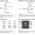

Leave a Reply