
You pull the MOSFET off the board and it’s got a dark scorch mark across the top, or the die has cracked, or it’s just quietly gone short from drain to source. Whatever the symptom, a burnt MOSFET is not a random event — it’s the end result of one specific stress the part couldn’t survive. The trick is figuring out which stress it was, because the fix for weak gate drive looks nothing like the fix for shoot-through in an H-bridge, and using the wrong fix means you’ll burn the replacement part too.
This guide walks through the nine most common causes of MOSFET failure — from under-driven gates to dried-out thermal paste — with the symptoms that point to each one and the specific fix.
Quick diagnosis: match your symptom to a cause
| Symptom | Most likely cause | Jump to |
|---|---|---|
| MOSFET runs hot even at low current, driven by a microcontroller pin | Insufficient gate drive voltage | Cause #1 |
| MOSFET fails right when switching, not while steady-on | Fast switching transients (high di/dt / dv/dt) | Cause #2 |
| Failure happens when driving a motor, relay, or solenoid | Motor back-EMF / flyback voltage | Cause #3 |
| Failure happens specifically during braking or when the motor is spun by an external load | Regenerative back-EMF (negative torque) | Cause #4 |
| Both high-side and low-side MOSFETs fail together, often with a loud pop | Shoot-through in an H-bridge or half-bridge | Cause #5 |
| You paralleled MOSFETs for more current, and now only one is charred | Current imbalance between parallel MOSFETs | Cause #6 |
| MOSFET fails during a voltage surge, load dump, or when tested above its rated voltage | Exceeding the VDS / supply voltage rating | Cause #7 |
| Board runs fine cold, MOSFET dies after 10–20 minutes | Heatsink misconnection or poor thermal contact | Cause #8 |
| An old, previously reliable design suddenly starts cooking MOSFETs | Dried-out thermal paste | Cause #9 |
Cause #1: Insufficient Gate Drive Voltage (Under-Vgs Drive)
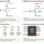
This is the single most common reason a mosfet gate driver question ends with a burnt part, and it’s almost always the same story: VCC or VDD are 3.3 V or 5 V microcontroller pin is wired straight to the gate of a standard-threshold MOSFET.
Every MOSFET datasheet lists an RDS(on) figure, but that number is only valid at a specific gate-source voltage — usually 10 V. Drive the gate with less than that, and the channel never fully enhances. The MOSFET sits in its linear region instead of full saturation, RDS(on) can be five to ten times higher than the datasheet figure, and power dissipation (P = I²R) climbs accordingly. The part isn’t failing because it’s a bad component — it’s failing because it’s being asked to act as a switch while actually behaving like a lossy resistor.
How to fix it:
- Check VGS(th) and the RDS(on) test condition in the datasheet before wiring anything to a logic pin.
- For 3.3 V/5 V logic, choose a logic-level MOSFET rated for full RDS(on) at that gate voltage, or add a dedicated gate driver IC between the microcontroller and the gate.
- A proper gate driver circuit also matters at the top end: it supplies the peak current needed to charge and discharge the gate capacitance quickly, which shortens the time spent in the lossy linear region during every switching transition — not just at DC.
- For high-side N-channel switching, you need a mosfet with gate driver support for bootstrapped or charge-pumped drive, since the gate has to be pulled cross the power rails VCC/VDD or VSS/ VEE.
If you haven’t already, it’s worth reading through a dedicated gate-driver walkthrough before you touch the rest of this list — under-drive is the root cause behind a large share of the failures described below too, because a MOSFET that’s already running hot from weak drive has far less margin left to survive a transient.
Cause #2: Fast Switching Transients — High di/dt and dv/dt
Even with perfect gate drive, every trace and component lead has parasitic inductance. When a MOSFET switches current off quickly, that stray inductance fights the change (V = L·di/dt) and produces a voltage spike on the drain that can exceed the part’s VDS rating for a few nanoseconds — long enough to push the MOSFET into avalanche breakdown repeatedly until it degrades and fails.
This failure mode is sneaky because it doesn’t show up as sustained heat. The MOSFET can run cool and still die, because the damage happens in short, repeated spikes at every switching edge rather than as continuous dissipation.
How to fix it:
- Keep the loop area between the MOSFET, the decoupling capacitor, and the load as small as physically possible — this is the single biggest lever on stray inductance.
- Add a snubber circuit across the drain-source (an RC or RCD network) to absorb the energy in the spike before it can push VDS past the rating. This is the same idea used in an RC/RCD snubber design for SCRs, just sized around the MOSFET’s own Coss and the loop inductance instead.
- Choose a MOSFET with enough avalanche energy rating (EAS) margin if repetitive avalanche is unavoidable in your topology, rather than relying on the part surviving avalanche indefinitely.
Cause #3: Motor Back-EMF and Flyback Voltage
Any mosfet motor driver circuit is switching current through an inductive load, and inductors resist sudden current changes. The instant you turn a motor-driving MOSFET off, the coil’s stored energy has to go somewhere — and without a path for it, it flies back as a large negative voltage spike on the drain, often well beyond the supply rail.
This is a different mechanism from Cause #2 (which comes from parasitic trace inductance): here the inductance is the motor winding itself, and the energy involved is much larger.
How to fix it:
- Always include a flyback (freewheeling) diode across the motor terminals in single-MOSFET low-side switching, sized for the motor’s peak current.
- In bridge topologies, the body diodes of the opposite MOSFETs usually provide this path — but only if they’re rated for the current and given time to conduct.
- Add a TVS diode or snubber if the flyback event still pushes VDS close to the rating even with a flyback diode present, which happens with long motor leads or brushed motors with high winding inductance.
Cause #4: Negative Torque / Regenerative Back-EMF
This one catches people off guard because it looks like Cause #3 but happens under the opposite condition: instead of the motor being driven, it’s being driven backward — spun by momentum, an external load, or braking — and the motor now acts as a generator feeding current back into the driver.
During regenerative braking or “negative torque” conditions, current flows in the reverse direction through what was the freewheeling path, and if the driver circuit or the DC bus can’t absorb that returned energy, the bus voltage rises until something exceeds its rating — usually the MOSFET that’s least protected in that direction. This is a common, underappreciated cause of MOSFET failure in BLDC and stepper motor drivers, robotics, and e-bike controllers, precisely because it only shows up during braking or coasting, not during normal forward drive — which is why the failure looks intermittent until you isolate the condition that triggers it.
How to fix it:
- Add bus capacitance sized for the regenerated energy, or a bleeder/brake resistor circuit to dump it as heat.
- Verify the DC bus voltage during a full-load braking event, not just during acceleration — this is the condition most designs never actually test.
- In H-bridge and three-phase drives, make sure the high-side body diodes and any freewheeling paths are rated for the full regenerated current, not just the forward drive current.
Cause #5: Shoot-Through in H-Bridge and Half-Bridge Drivers
If you’re running a mosfet driver h bridge or any half-bridge topology and MOSFETs are failing in matched pairs — often with a loud pop and a blown fuse or trace — the most likely cause is shoot-through: the high-side and low-side MOSFETs conducting at the same time, even briefly, which creates a near dead-short across the supply rail.
Shoot-through in a mosfet hbridge usually comes from one of two places: insufficient dead-time between turning one MOSFET off and the other on, or a MOSFET that turns on unintentionally because a fast dV/dt edge on its drain couples through the gate-drain (Miller) capacitance and pulls the gate above threshold even though it was supposed to be off.
How to fix it:
- Use a dedicated half-bridge or H-bridge gate driver IC with built-in dead-time and interlock protection rather than driving four MOSFETs from raw GPIO logic.
- If designing your own mosfet h bridge design from discrete drivers, add explicit dead-time in firmware or hardware — err on the side of too much dead-time while debugging, then tighten it once the circuit is proven stable.
- Add a gate-source pulldown resistor and keep gate traces short to reduce susceptibility to Miller-induced false turn-on.
Cause #6: Current Imbalance Between Parallel MOSFETs
Paralleling MOSFETs to handle more current seems straightforward — split the current across two or more parts, and each one runs cooler. In practice, MOSFETs rarely share current evenly, and a parallel mosfet gate driver setup that doesn’t account for this will eventually lose one MOSFET, and often take the rest with it.
The failure cascades because of RDS(on)’s positive temperature coefficient: if one MOSFET happens to have slightly lower RDS(on) or turns on slightly faster, it carries more current, which makes it run hotter, which raises its RDS(on) further — but not enough to correct the imbalance before it overheats and fails short. Once one MOSFET is gone, the remaining ones inherit its full share of the current and fail in sequence.
How to fix it:
- Match MOSFETs from the same batch when paralleling, and add small individual gate resistors on each part to slow and desynchronize their switching slightly, which improves current sharing during transitions.
- Use Kelvin source connections where the layout allows, so each MOSFET’s gate drive reference isn’t distorted by shared source inductance.
- Keep drain and source trace lengths symmetric between the paralleled parts — asymmetric layout is one of the most common hidden causes of current imbalance.
Cause #7: Exceeding the VDS / Supply Voltage Rating
Sometimes the cause is the simplest one on this list: the MOSFET’s rated VDS is lower than what the circuit can actually present, whether from a load dump, an input voltage surge, a battery pack briefly exceeding nominal, or — combined with Cause #2 or #3 — a spike stacked on top of an already-high rail.
A high voltage gate driver and a high-voltage-rated MOSFET are not the same design decision — the driver handles the gate-side switching correctly, but the MOSFET itself still needs enough margin between its VDS rating and the highest transient voltage the drain will ever see, not just the nominal supply.
How to fix it:
- Pick a MOSFET with VDS rated comfortably above the highest transient the rail can produce, not just the steady-state supply voltage — a common rule of thumb is 20–30% headroom minimum, more if the source is unregulated or battery-based.
- Add transient/surge protection (TVS diode, clamp) at the supply input if the source itself is the problem, rather than over-specifying every MOSFET downstream.
Cause #8: Heatsink Misconnection and Poor Electrical/Thermal Contact
This cause produces a very specific symptom: the circuit works fine for the first several minutes, then the MOSFET fails once it’s had time to heat up — because the heat sink design for mosfet packages like TO-220 or TO-247 has a subtlety that’s easy to miss. On most N-channel power MOSFETs, the metal tab is electrically connected to the drain, not electrically isolated. Bolt it straight to a shared metal heatsink with other components, and you can either short the drain to another device’s tab or — more relevant here — fail to achieve proper thermal contact because an insulating pad was installed incorrectly, is the wrong thickness, or is missing entirely.
How to fix it:
- Confirm whether the package tab is electrically live (check the datasheet’s pinout diagram) before deciding whether an insulating thermal pad is required.
- Use the correct insulating pad type and torque spec for the mounting screw — too little clamping force leaves an air gap that ruins thermal transfer even with a good pad.
- Run a mosfet heat sink calculator using your actual power dissipation (from Cause #1’s RDS(on) math) and the heatsink’s thermal resistance to confirm the junction temperature actually stays in a safe range under worst-case load, rather than assuming “a heatsink” is enough.
Cause #9: Dried-Out or Poorly Applied Thermal Paste
Related to Cause #8 but distinct: this is the failure that shows up in a design that used to work. Thermal paste (thermal interface material) fills the microscopic air gaps between the MOSFET package and the heatsink, and most standard pastes degrade over months to years — drying out, cracking, or pumping out from thermal cycling. As the interface degrades, thermal resistance climbs, junction temperature climbs with it, and a MOSFET that had been running with healthy margin for years can start failing with no other change to the circuit.
How to fix it:
- If an established design suddenly starts failing MOSFETs with no circuit changes, check thermal paste condition before suspecting the electrical design at all.
- Reapply paste with a thin, even layer — too much is nearly as bad as too little, since excess paste squeezes out unevenly and can leave thicker regions than a properly applied thin layer would.
- For high-reliability or high-temperature applications, consider a paste rated for the expected thermal cycling, rather than a general-purpose one intended for lower-duty electronics.
Diagnosing Which MOSFET Problem You Actually Have
Mosfet problems rarely announce themselves with a label. A few quick checks narrow it down fast:
- Measure gate voltage during operation, not just at the source. If it’s below the datasheet’s RDS(on) test voltage, start with Cause #1.
- Scope the drain during a switching transition, not just at steady state. A sharp spike above the rail points to Cause #2 or #3 depending on whether the load is resistive or inductive.
- Check whether the failure correlates with braking, coasting, or reverse rotation in motor applications — that’s the signature of Cause #4, not #3.
- Check whether both sides of a bridge failed together — near-simultaneous failure across a half-bridge is close to diagnostic for shoot-through (Cause #5).
- Feel the heatsink temperature at the point of failure, if you can reproduce it slowly — a heatsink that’s barely warm while the MOSFET is cooking points to a thermal interface problem (Cause #8 or #9), not an electrical one.
A Basic MOSFET Protection Circuit Checklist
A reasonable baseline mosfet protection circuit design for anything beyond a simple low-power switch includes:
- A gate driver (discrete or IC) sized for the gate charge and switching frequency, not a bare GPIO pin.
- A gate-source pulldown resistor to hold the gate off during power-up and MCU reset.
- A flyback diode or snubber across any inductive load.
- A MOSFET voltage rating with real margin above the highest transient the rail can produce.
- Thermal design verified with actual power dissipation numbers, not assumed “close enough.”
None of these individually is exotic, but skipping any one of them is how a design that works on the bench starts failing in the field.
FAQ
Can a MOSFET fail without shorting? Yes. MOSFETs can fail open, fail short, or degrade partially (elevated RDS(on) without full failure). Repeated avalanche stress (Cause #2) and thermal degradation often cause partial degradation before a full short or open failure.
How hot is too hot for a MOSFET? It depends on the part’s rated junction temperature (commonly 150°C or 175°C), but the case temperature you can safely touch is much lower than that — a MOSFET can be well past a safe operating point while still feeling “just warm” to the hand, because junction temperature runs higher than case temperature under load. Use the datasheet’s thermal resistance figures rather than touch as a test.
Why does my MOSFET work fine cold but fail once the circuit’s been running a while? This points to a thermal cause — either Cause #1 (under-drive raising RDS(on) and heat over time), Cause #8 (poor heatsink contact), or Cause #9 (degraded thermal paste) — rather than a voltage-transient cause, which would typically fail quickly or not at all.
Do I need a snubber if I already have a flyback diode? Often yes, for different reasons. A flyback diode handles the bulk energy from an inductive load turning off; a snubber handles the much faster ringing caused by parasitic inductance and MOSFET output capacitance at the switching edge itself. Fast-switching or high-frequency designs frequently need both.
Related reading on this site: see the gate-driver interfacing guide for direct-drive and high-side switching circuits, and the snubber circuit design guide for RC/RCD sizing — the same snubber principles apply directly to protecting a MOSFET’s drain-source voltage during switching.




Leave a Reply