
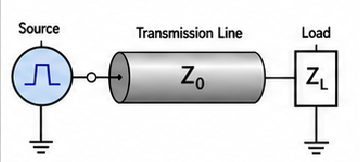
In modern electronics, a signal is not just a voltage traveling from one point to another. it is the carrier of information. Whether in a simple LED circuit or a high-speed communication system, maintaining the integrity of that signal is critical. However, in real-world systems, signals rarely behave ideally. They degrade, distort, and interact with their environment. This is where signal integrity becomes a fundamental engineering concern.
This article focuses specifically on wired systems, including cables, PCB traces, and interconnects. Unlike wireless systems, where signals propagate through space, wired systems involve physical conductors where electromagnetic effects, impedance, and coupling dominate behavior. Understanding these effects is essential for designing reliable electronic systems.
What is Signal Integrity?
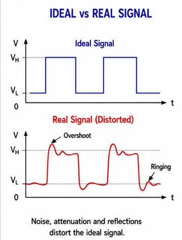
Signal integrity refers to the quality and reliability of an electrical signal as it travels through a medium. An ideal signal would maintain its original shape, amplitude, and timing. In practice, however, signals are affected by noise, losses, reflections, and interference.
A useful way to understand this is to consider a signal as a combination of three components:
Signal = Information + Carrier + Noise
The goal of signal integrity design is to preserve the information while minimizing distortion introduced by the transmission medium.
What is a Signal? Physical Perspective
At a fundamental level, a signal is a time-varying voltage or current that represents information. In digital systems, signals switch between discrete levels, while in analog systems, they vary continuously. Regardless of type, every signal exists within a physical system governed by electromagnetic laws.
In theory, signals are often represented as ideal waveforms. In reality, every signal is subject to distortion due to the properties of the medium through which it travels. These distortions become more pronounced as frequency increases or as physical dimensions grow relative to wavelength.
Why Real Wires Are Not Ideal
In basic circuit theory, wires are often treated as perfect conductors with zero resistance and no parasitic effects. This assumption fails in practical systems. Every conductor exhibits distributed electrical properties that affect signal behavior.
A real interconnect can be modeled using distributed parameters:
R, \; L, \; C, \; G
Where:
R represents resistance, causing power loss and voltage drop.
L represents inductance, associated with magnetic fields and current changes.
C represents capacitance between conductors, storing electric energy.
G represents conductance, modeling leakage through insulating materials.
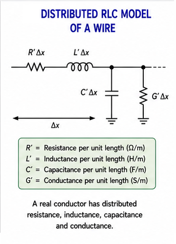
These parameters are not lumped at a single point—they are distributed along the length of the conductor. This distributed nature leads to complex behaviors that cannot be explained using simple circuit models.
When a Wire Becomes a Transmission Line
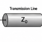
A critical transition occurs when the physical length of a conductor becomes comparable to the wavelength of the signal. At this point, the wire no longer behaves as a simple connection—it becomes a transmission line.
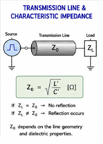
The characteristic impedance of a transmission line is defined as:
Z_0 = \sqrt{\frac{L}{C}}This impedance determines how signals propagate and how reflections occur at discontinuities. Mismatches between source, line, and load impedance result in reflected waves, which distort the original signal.
Understanding transmission line behavior is essential for high-speed digital design, RF systems, and long cable runs. In later sections, we will connect this concept to practical systems such as twisted pair cables and PCB traces.
Sources of Signal Degradation
As signals propagate through real-world interconnects, they encounter multiple degradation mechanisms. These effects are interconnected and often occur simultaneously.
Noise arises from external electromagnetic interference (EMI) and internal circuit activity.
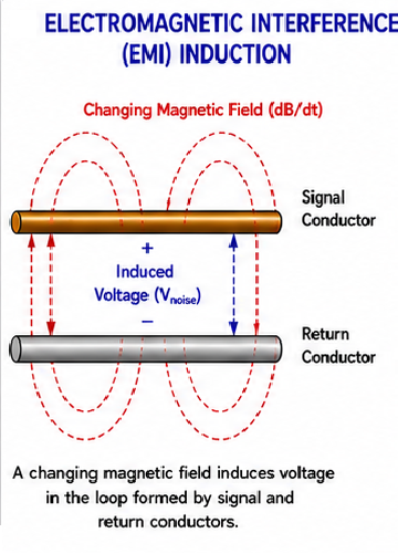
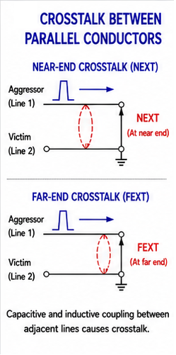
Crosstalk occurs when signals in adjacent conductors couple through electric or magnetic fields.
Reflection results from impedance mismatches, causing part of the signal to travel back toward the source.
Attenuation reduces signal amplitude due to resistive and dielectric losses.
Each of these mechanisms will be explored in dedicated articles, with detailed mathematical modeling and design techniques.
The Importance of Return Current Path
One of the most misunderstood aspects of signal integrity is the concept of the return current path. In many introductory explanations, current is assumed to flow through a “ground wire.” In reality, current always follows the path of least impedance, which depends on frequency and electromagnetic field distribution.
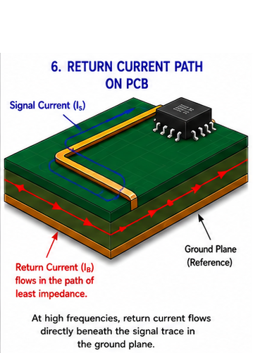
At high frequencies, return current tends to flow directly beneath the signal conductor, following the path that minimizes loop area. This behavior has critical implications for PCB design, grounding strategies, and electromagnetic emissions.
A poor return path increases loop area, leading to higher inductance, increased noise susceptibility, and greater radiation. This concept forms the foundation for advanced PCB design techniques and will be explored in depth in later articles.
Single-Ended vs Differential Signaling
In wired systems, signals can be transmitted using either single-ended or differential methods. Understanding the distinction between these two approaches is fundamental to modern signal integrity design.
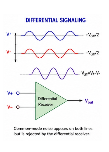
In single-ended signaling, a signal is referenced to a common ground. The receiver measures the voltage of the signal line relative to this reference. While simple, this method is highly susceptible to noise, especially when the ground reference is unstable or contaminated by switching currents.
In contrast, differential signaling uses two conductors carrying equal and opposite signals. The receiver detects the difference between these two voltages, effectively rejecting noise that appears equally on both lines.
V_{diff} = V^{+} - V^{-}This configuration provides strong immunity to external interference and is widely used in high-speed systems such as Ethernet, USB, and modern digital interfaces.
Detailed mathematical treatment of common-mode rejection and noise cancellation will be covered in the dedicated article on differential signaling.
Role of Twisted Pair in Noise Reduction
Twisted pair cables are one of the most effective and widely used solutions for maintaining signal integrity in wired systems. Their effectiveness is rooted in electromagnetic field behavior rather than simple wiring convenience.
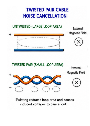
When two conductors are twisted together, the electromagnetic fields they generate alternate positions along the cable length. This periodic inversion causes induced noise to cancel over distance, significantly reducing susceptibility to external interference.
From a physical perspective, twisting reduces the loop area between conductors. Since induced voltage is proportional to the rate of change of magnetic flux through this loop, minimizing the loop area directly reduces noise pickup.
V = \frac{d\Phi}{dt}This principle makes twisted pair cables highly effective for differential signaling, where both conductors experience nearly identical interference that is later canceled at the receiver.
Advanced topics such as twist rate optimization, crosstalk reduction, and cable construction (UTP, STP, FTP) will be explored in dedicated articles.
Electromagnetic Shielding in Wired Systems
While twisting reduces susceptibility to noise, it does not eliminate all forms of interference. In environments with strong electromagnetic fields, additional protection is required. This is achieved through electromagnetic shielding.
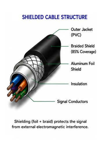
Shielding works by either reflecting or absorbing electromagnetic energy before it can couple into the signal conductors. Conductive materials such as copper or aluminum are commonly used to form barriers around cables or PCB traces.
The effectiveness of shielding depends on material properties, thickness, frequency, and proper grounding. Poorly grounded shields can act as antennas, worsening interference instead of reducing it.
In cable systems, shielding appears in various forms such as foil shields, braided shields, or combinations of both. In PCB design, shielding is implemented using ground planes, guard traces, and enclosure design.
A deeper analysis of shielding effectiveness, including skin effect and transfer impedance, will be covered in the dedicated shielding section.
Signal Integrity in PCB Traces vs Cables
Although cables and PCB traces appear physically different, they obey the same electromagnetic principles. Both act as transmission lines when operating at sufficiently high frequencies.
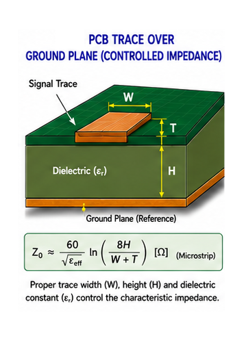
In cables, geometry is fixed and controlled during manufacturing. In contrast, PCB traces are designed by engineers, allowing precise control over impedance, spacing, and return paths.
Key similarities include:
Both exhibit distributed resistance, inductance, and capacitance.
Both require impedance matching to prevent reflections.
Both are affected by crosstalk and electromagnetic interference.
Understanding this equivalence allows engineers to apply the same theoretical framework across cables and PCB designs, simplifying analysis and improving system reliability.
Real-World Engineering Examples
Signal integrity principles are not abstract—they directly impact real-world systems. Consider the following examples:
In Ethernet communication, twisted pair cables are used to transmit high-speed differential signals while minimizing noise and crosstalk.
In USB and high-speed digital interfaces, differential pairs on PCBs ensure reliable data transfer at high frequencies.
In power electronics, improper grounding and return paths can introduce noise that disrupts sensitive control circuits.
These examples illustrate that signal integrity is not optional—it is a fundamental requirement for modern electronic design.
Concept Map of Wired Signal Integrity
Signal Integrity
 ├── Transmission Lines
 ├── Twisted Pair
 ├── Differential Signaling
 ├── Shielding
 ├── PCB Design
 └── Return Current
This conceptual structure forms the foundation of all subsequent articles. Each branch represents a deep area of study that will be explored individually with mathematical models, design rules, and practical implementations.
Related Topics to Explore
To build a complete understanding of wired signal integrity, the following topics should be explored in detail:
- Twisted Pair Cable Theory
- Differential Signaling and Noise Rejection
- Transmission Line Fundamentals
- Electromagnetic Shielding Techniques
- PCB Grounding and Return Current Paths
Each of these topics will be developed as standalone articles and interconnected to form a comprehensive knowledge network.
Frequently Asked Questions (FAQ)
What is signal integrity in wired systems?
Signal integrity refers to the ability of a signal to maintain its original shape, timing, and amplitude as it travels through cables or PCB traces without distortion or noise interference.
Why do signals degrade in wires and PCB traces?
Signals degrade due to resistance, inductance, capacitance, electromagnetic interference, reflections from impedance mismatches, and crosstalk between nearby conductors.
What is the difference between single-ended and differential signaling?
Single-ended signaling uses one signal line referenced to ground, while differential signaling uses two complementary signals and measures their difference, providing better noise immunity.
Why are twisted pair cables used in communication systems?
Twisted pair cables reduce electromagnetic interference by alternating the position of conductors, which cancels induced noise and minimizes loop area.
What is a transmission line and when does it matter?
A transmission line is a conductor where signal behavior is governed by distributed parameters. It becomes important when the signal wavelength is comparable to the physical length of the conductor.
What is the return current path in signal integrity?
The return current path is the route through which current completes its loop. At high frequencies, it follows the path of least impedance, typically directly beneath the signal trace.
Conclusion
Signal integrity in wired systems is not an optional consideration—it is a fundamental requirement for reliable electronic design. As signals travel through cables and PCB traces, they interact with the physical world, encountering resistance, inductance, capacitance, and electromagnetic fields. These interactions shape how signals behave and determine whether information is transmitted accurately or lost in distortion.
From the distributed nature of interconnects to the transition into transmission line behavior, and from noise sources to return current paths, every aspect of signal integrity is interconnected. Techniques such as differential signaling, twisted pair design, and electromagnetic shielding are not isolated solutions—they are part of a unified framework that governs signal behavior in real systems.
Understanding these principles provides a strong foundation for advanced topics, including high-speed PCB design, impedance control, and electromagnetic compatibility. As electronic systems continue to operate at higher speeds and greater complexity, mastering signal integrity becomes increasingly essential.
Explore Next Topics
To deepen your understanding, continue with the following advanced topics that expand on the concepts introduced in this article:
- Twisted Pair Cable: Electromagnetic Theory and Noise Cancellation
- Differential Signaling: Noise Immunity and High-Speed Design
- Transmission Line Theory: Impedance, Reflection and Matching
- Electromagnetic Shielding: Principles and Practical Implementation
- PCB Grounding and Return Current Path Design
These articles are interconnected and will collectively build a comprehensive understanding of wired signal integrity and interconnect engineering.



Leave a Reply